Optically isolated bias control circuit

a bias control circuit and optically isolated technology, applied in the field of optically isolated bias control circuits, can solve the problems of low frequency of useful operation, large and heavy transformers capable of low frequency operation, and high cost of high-voltage transformers designed to isolate high-voltage voltages, so as to reduce the flow of charge, and reduce the effect of rise and fall times

Inactive Publication Date: 2004-12-23
THE UNITED STATES OF AMERICA AS REPRESETNED BY THE SEC OF THE AIR FORCE
View PDF6 Cites 27 Cited by
  • Summary
  • Abstract
  • Description
  • Claims
  • Application Information

AI Technical Summary

Benefits of technology

0032] Referring to FIG. 1, a schematic of the present invention is shown. This preferred embodiment of the present invention comprises a floating bias voltage source 100 positive terminal electrically connected in series to the collector of a photo-transistor (Q1) 110. The emitter of Q1 110 is connected in series through inductance (L) 120 to the parallel connected N-channel enhancement-mode MOSFET 130 gate (G) and collector of another photo-transistor (Q2) 140. The emitter of Q2 140 is connected to both the MOSFET source (S) and to the negative terminal of the bias voltage source. The bias voltage source 100 may be either a solar power source or a battery, and with its positive voltage terminal electrically connected in series with a diode D1 150 (for solar source) to a parallel connected energy storage capacitor (C1) 160 and low inductance capacitor (C2) 170 which are series connected to the negative voltage terminal of the bias voltage source 100 (solar powered source or battery). Operation of this embodiment of the present invention requires the illumination of the solar powered source or connection to a battery to achieve the operating voltage across the energy storage capacitor C1 160. When the operating voltage is reached, two complementary "ON" and "OFF" light signal pulses are applied to the light sensitive base regions of the photo-transistors Q1 110 and Q2 140, respectively. Minimal charge flow is achieved by allowing the active high "ON" light signal to be applied in the high state to photo-transistor Q1 110 only when the active high "OFF" light signal applied to photo-transistor Q2 140 is in the low state (see FIG. 3 "TIMING DIAGRAM"). This prevents the direct shorting of the bias voltage source 100 (solar power source or battery) through both photo-transistors 110, 140 and reduces the flow of charge required to control the MOSFET 130 switching circuit. It is important to apply "ON" and "OFF" light signal pulses which have minimal rise and fall times to ensure that the MOSFET 130 is driven as fast as possible through its switching states. Darlington photo-transistors may be used to reduce the rise and fall times of the control pulses. This decreases the time in which the MOSFET 130 has drain-to-source resistances which can dissipate heat (waste energy), cause the device temperature to increase and possibly damage the MOSFET 130. It is important to note that the stray capacitance of photo-transistor (Q2) 140 together with the MOSFET 130 gate capacitance, inductances of the source and drain, and Miller effects will affect the efficiency of operation as a function of frequency and the range of effective switching pulse widths and duty cycles. Switched capacitor circuits can dissipate energy by radiation and generate electromagnetic noise. A properly selected small inductance (L) 120 in series with the gate can reduce switching losses by appropriately slowing the gate capacitor charging time.

Problems solved by technology

Disadvantages of simple transformer biasing include a lower limit to the frequencies of useful operation (this precludes DC operation), pulse transformers designed to isolate high voltages can be expensive and unreliable, and transformers capable of low frequency operation are large and heavy.

Method used


Image

  • Optically isolated bias control circuit
  • Optically isolated bias control circuit
  • Optically isolated bias control circuit

Examples


embodiment # 1

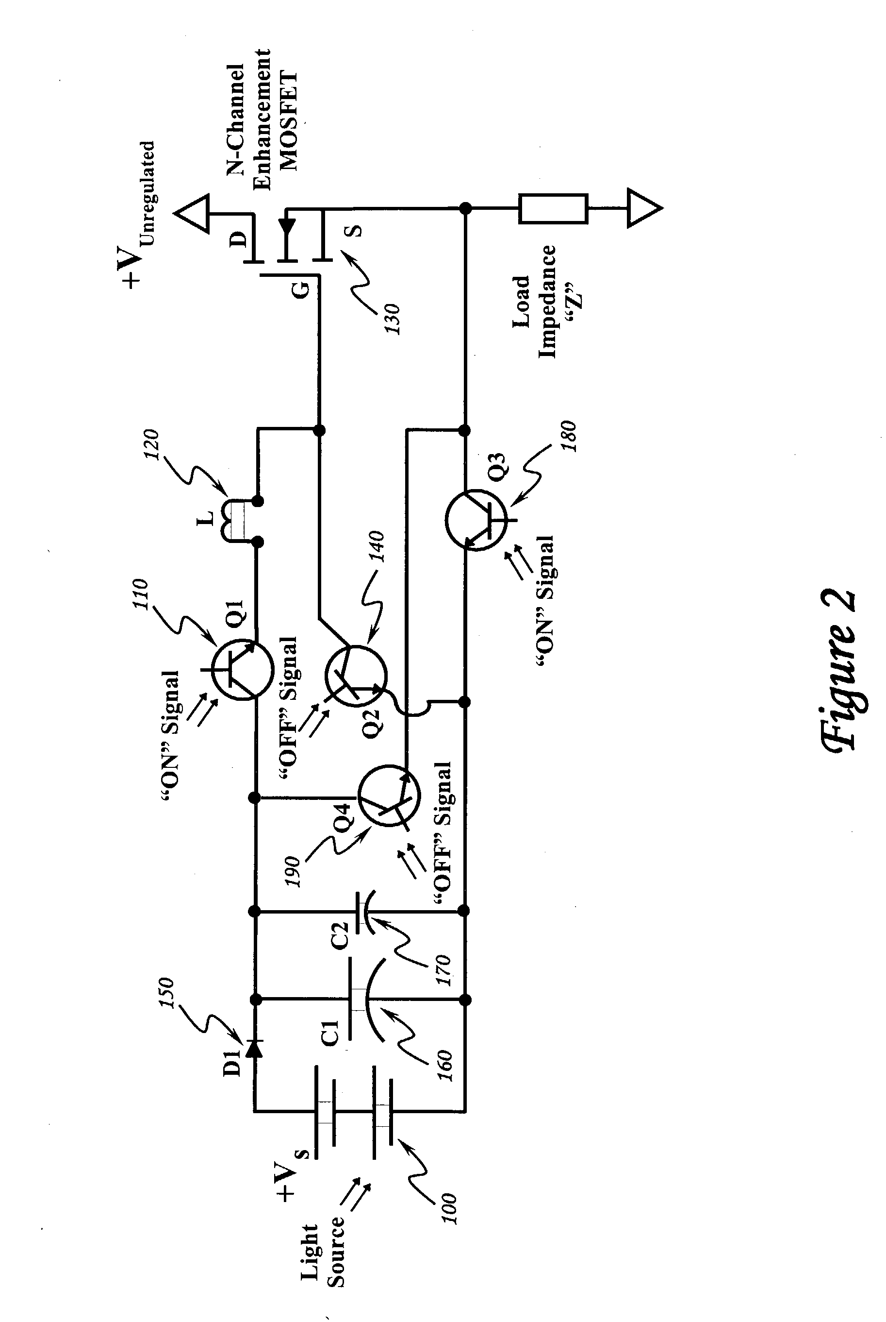
[0033] Alternate Embodiment #1

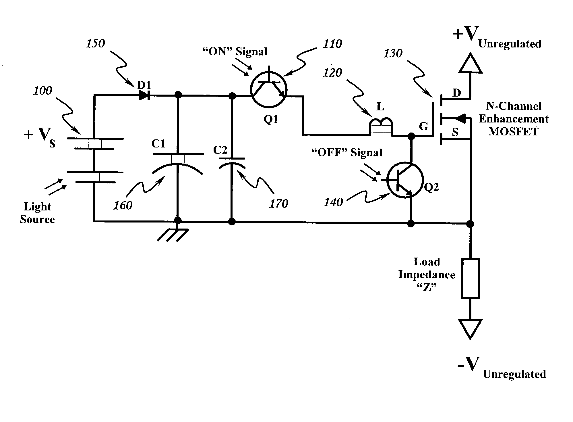
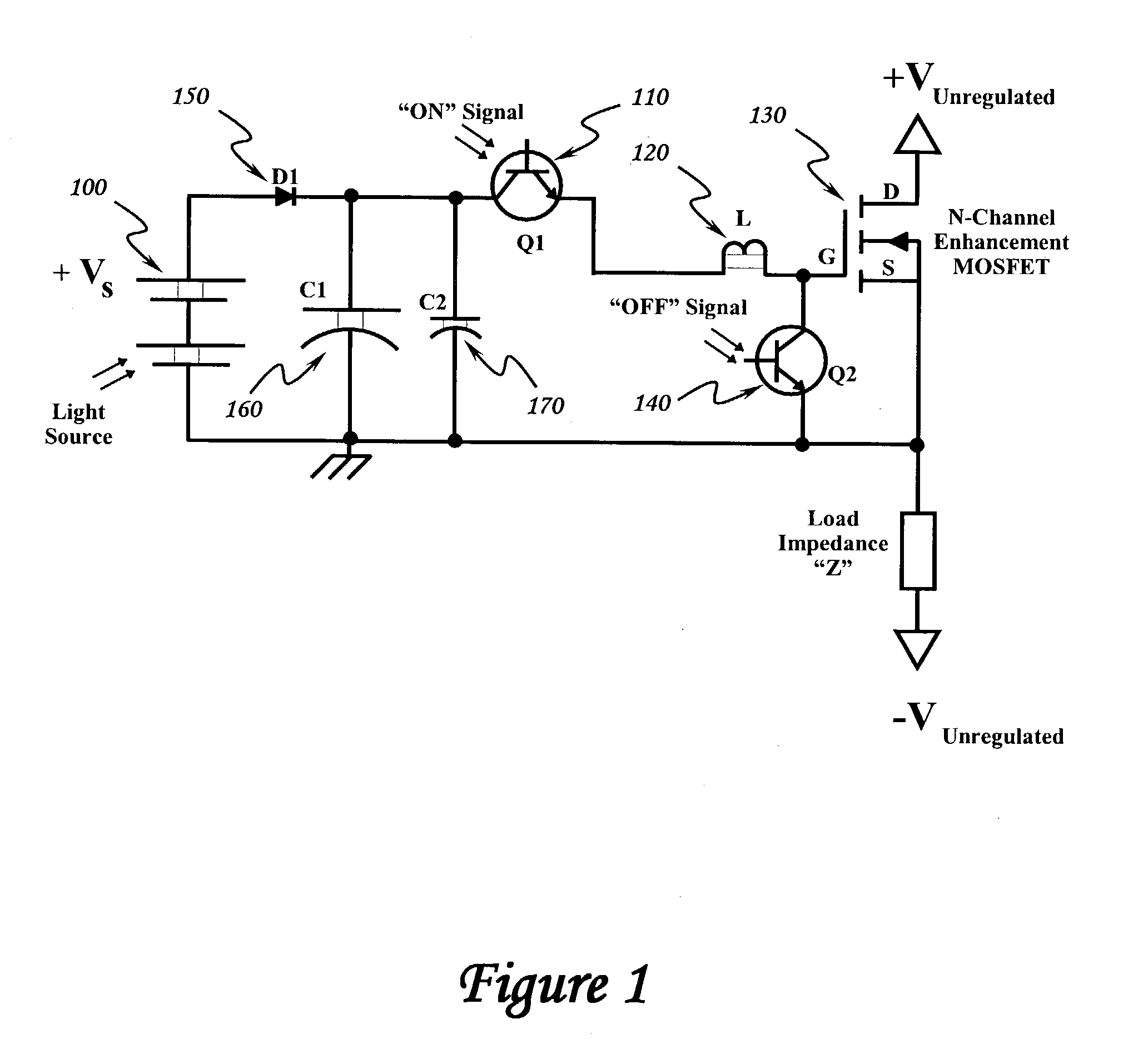
[0034] Referring to FIG. 2, a first alternative embodiment of the invention is depicted. The first alternate embodiment of the present invention involves the use of two additional optically isolating photo-transistors Q3 180 and Q4 190. This embodiment effectively reverses the polarity of the bias voltage source 100 applied to the gate-to-source circuit of the MOSFET 130 in order to force the circuit off as fast as it is forced on. This circuit has enhanced noise immunity due to a negative gate-to-source voltage and may be able to operate with pulses of faster rise and fall times than the embodiment depicted in FIG. 1 with a given gate control voltage, but it requires two additional optically isolating devices.

[0035] Referring to FIG. 4, a series connection of either embodiment of the gate bias control circuits (see FIG. 1 or FIG. 2) is depicted that enables operating voltages greater than a single MOSFET can hold off. The series of gate bias control ci...


PUM


Abstract

Optically isolated bias control circuit which provides bias current for switching circuits. Invention is amenable to high speed switching control with instantaneously variable pulse widths and duty cycles. Invention can be operated from DC upward in frequency, limited only by the characteristics of the implementing electrical components and electrical interconnections. Complementary embodiments of invention provide high speed operation with minimal electrical charge flow. Solar powered embodiments of invention may be used to control the switching of high power MOSFET-based switching circuits.

Description

[0002] A common method of controlling a MOSFET in "high-side" connected circuits requires the use of a voltage isolating pulse transformer in the gate-to-source biasing circuit. "High-side" refers to a circuit configured with the MOSFET switch connected between the supply voltage and the load impedance; it is connected to the higher voltage side of the load impedance. A "low-side" connected MOSFET does not, typically, present damaging gate-to-source voltages, but then one end of the load impedance is connected to the high side of the supply voltage. A voltage isolating pulse transformer can be used in "high-side" circuits; it allows the gate-to-source circuit to float (electrically) near the source potential which prevents the gate-to-source voltage from reaching device damaging values. Disadvantages of simple transformer biasing include a lower limit to the frequencies of useful operation (this precludes DC operation), pulse transformers designed to isolate high voltages can be exp...

Claims


Application Information

Patent Timeline
Patent Type & Authority Applications(United States)
IPC IPC(8): G02B27/00H03F1/30H03F3/08H03F17/00
CPCH03F1/303H03F3/082H03K17/04123H03K17/162H03K17/785
Inventor MCEWEN, THOMAS A.
Owner THE UNITED STATES OF AMERICA AS REPRESETNED BY THE SEC OF THE AIR FORCE
Why Eureka
Try Eureka