Nonvolatile semiconductor memory device, and programming method and erasing method thereof

Active Publication Date: 2004-12-23
XENOGENIC DEV LLC
View PDF15 Cites 42 Cited by
  • Summary
  • Abstract
  • Description
  • Claims
  • Application Information

AI Technical Summary

Problems solved by technology

As shown in FIG. 2, however, in the case where a memory cell is formed of a cell selecting element made up of a transistor and a variable resistive element, only a slight problem occurs regarding `disturbance` (error programming, error erasing and the like) of the unselected memory cells, which are not to be programmed or erased, si

Method used


Image

  • Nonvolatile semiconductor memory device, and programming method and erasing method thereof
  • Nonvolatile semiconductor memory device, and programming method and erasing method thereof
  • Nonvolatile semiconductor memory device, and programming method and erasing method thereof

Examples


first embodiment

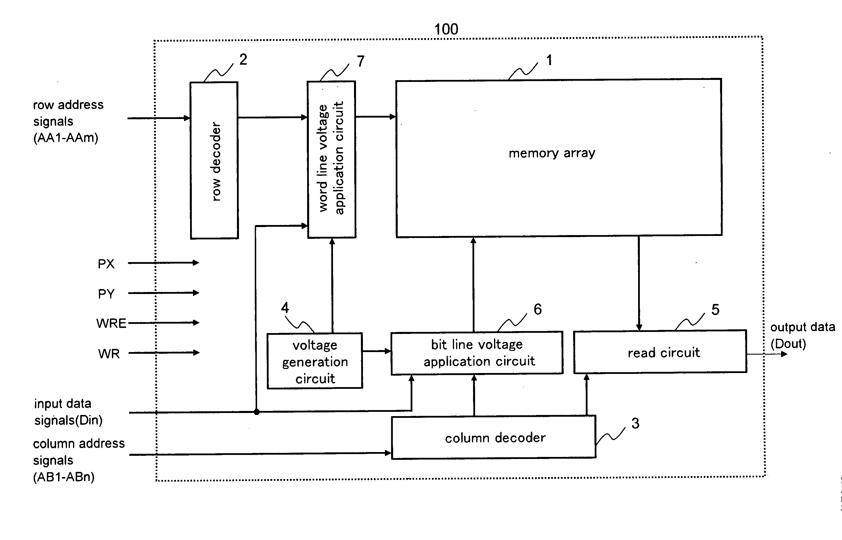
[0037] FIG. 3 is a block configuration diagram showing a functional configuration according to the inventive device. As shown in FIG. 3, an inventive device 100 is formed of a memory array 1, a row decoder 2, a column decoder 3, a voltage generation circuit 4, a read circuit 5, a bit line voltage application circuit 6 and a word line voltage application circuit 7.

[0038] FIG. 4 is a diagram showing the configuration of the memory array 1 of FIG. 3. The memory array 1 is provided with d word lines 20, e bit lines 21 and d.times.e memory cells. Each memory cell has a variable resistive element 22 at a portion where a bit line and a word line cross. One end of the variable resistive element 22 of each memory cell in the same row is connected to the same word line, and the other end of the variable resistive element 22 of each memory cell in the same column is connected to the same bit line. As shown in FIG. 4, no memory cells have a cell selecting element and therefore, the area of the ...

second embodiment

[0069] In the first embodiment, the voltage is applied to all variable resistive elements 22 that form the memory array 1 so that a current flows through the entirety of the memory cells; therefore, consumed power increases when the memory array becomes large in scale. In addition, as described in the first embodiment, it becomes difficult for the read circuit to determine the program state and the erase state when the number of word lines increases. Therefore, the configuration, in which the memory array 1 is divided so that the divided memory arrays are driven, is shown in a second embodiment.

[0070] FIG. 16 is a block configuration diagram showing a function configuration according to the second embodiment of an inventive device 200. In the second embodiment, the memory array 1 in the first embodiment is divided into a plurality of sub-arrays 201 so that each sub-array 201 can be accessed. FIG. 16 shows an example of a case wherein a 64 k bit memory having 8 bits for the row addre...


PUM


Abstract

One end of each variable resistive element, which forms a memory array, in the same row is connected to the same word line and the other end of each variable resistive element in the same column is connected to the same bit line. A first word line voltage is selected and applied to the selected word line, a second word line voltage is selected and applied to the unselected word lines, a first bit line voltage is selected and applied to the selected bit line, and a second bit line voltage is selected and applied to the unselected bit lines. The voltage difference between the first word line voltage and the first bit line voltage is set at a value that is no less than the first voltage difference that changes the resistance value of a variable resistive element, and the voltage difference between the first word line voltage and the second bit line voltage, the voltage difference between the second word line voltage and the first bit line voltage and the voltage difference between the second word line voltage and the second bit line voltage are respectively set at a value that is no greater than the second voltage difference that does not change the resistance value of a variable resistive element.

Description

[0001] 1. Field of the Invention[0002] The present invention relates to a nonvolatile semiconductor memory device having a variable resistive element, which stores data due to a change in the electrical resistance through the application of voltage, on a semiconductor substrate.[0003] 2. Description of the Related Art[0004] A technique of changing the resistance value of a material having a perovskite structure, at room temperature in a reversible manner by applying a voltage pulse to the material, which is known as a colossal magnetoresistance (CMR), is disclosed in U.S. Pat. No. 6,204,139, wherein the resistance value can be changed by a magnitude of ten times or more in a reversible manner through the application of a voltage pulse. FIG. 1 shows an example of the programming characteristics of this variable resistive element. As shown in FIG. 1, the resistance value of the variable resistive element changes depending on the magnitude of the program voltage. The resistance value c...

Claims


Application Information

Patent Timeline
IPC IPC(8): G11C11/15G11C13/00G11C16/28H01L27/10
CPCG11C13/0007G11C13/0069G11C16/3427G11C2013/009G11C2213/31G11C2213/77G11C13/0026G11C13/0028G11C16/10
Inventor TAMAI, YUKIOINOUE, KOHJIMORITA, TERUAKI
Owner XENOGENIC DEV LLC
Why Eureka
Try Eureka