Dual damascene interconnect structures having different materials for line and via conductors

Active Publication Date: 2004-12-30
AURIGA INNOVATIONS INC
View PDF6 Cites 13 Cited by
  • Summary
  • Abstract
  • Description
  • Claims
  • Application Information

AI Technical Summary

Benefits of technology

[0007] It is therefore an object of this invention to provide a method for improving the strength of vias that are fabricated in low-k dielectric materials. This and other objects are accomplished by use of the methods of the present invention. In one aspect, an interconnect structure formed on a substrate is disclosed. The structure comprises: a first layer of a first dielectric material having at least one first conductor embedded therein, the first conductor having a top surface coplanar with a top surface of the layer of dielectric material; and a second layer of a second dielectric material overlying the first layer of dielectric material and having at least one second conductor embedded therein. The second conductor comprises at least one first portion and at least one second portion, the second portion being formed of a material different from the first portion, wherein the first portion is in electrical contact with the first conductor, the second portion is overlying and in electrical contact with the first portion, the second portion has a lateral extent greater than that of the first portion, and the second portion has a top surface coplanar with a top surface of the second layer of dielectric material. Optionally, the interconnect structure further comprises: a first conductive liner disposed between the first portion and the second dielectric material and between the first portion and the first conductor; and a second conductive liner disposed between the second portion and the second dielectric material and between the second portion and the first portion, the second liner being formed of a material different from the first liner.

Problems solved by technology

Significant stresses can develop in the structure due to thermal expansion mismatches with the substrate and the metal interconnects.
These stresses can cause fatigue of copper vias or studs during thermal cycling, resulting in yield or reliability problems.
This series of single damascene steps is time-consuming and expensive.
Moreover, two separate layers of dielectric (via-level and line-level) exhibit inferior electrical characteristics as compared to a single layer of dielectric material such as that found in a typical dual damascene structure.

Method used


Image

  • Dual damascene interconnect structures having different materials for line and via conductors
  • Dual damascene interconnect structures having different materials for line and via conductors
  • Dual damascene interconnect structures having different materials for line and via conductors

Examples


first embodiment

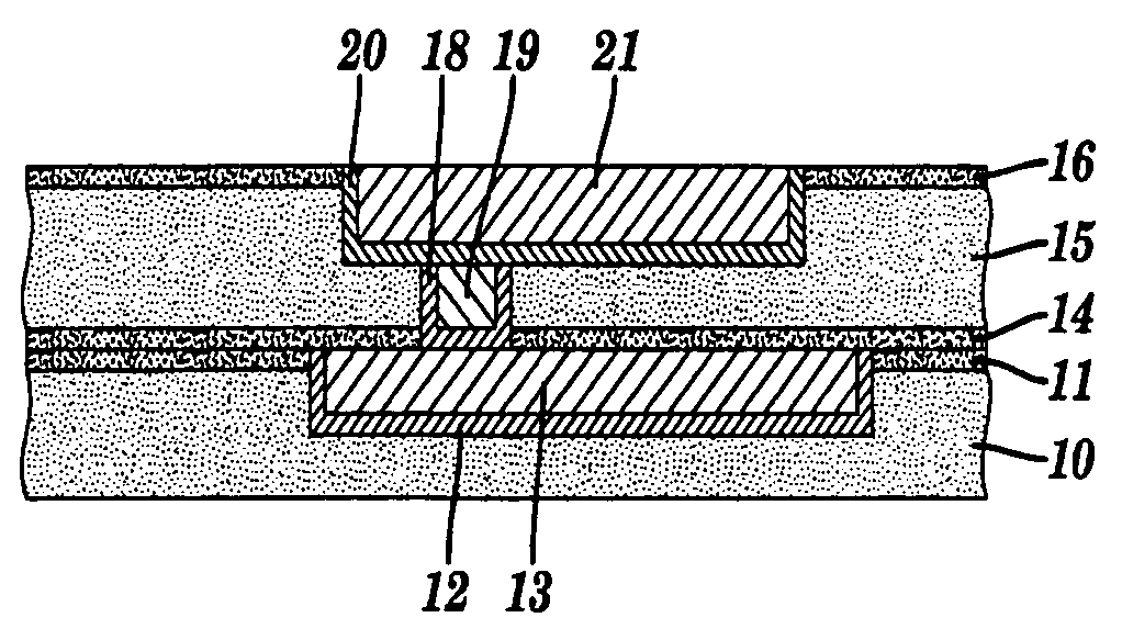
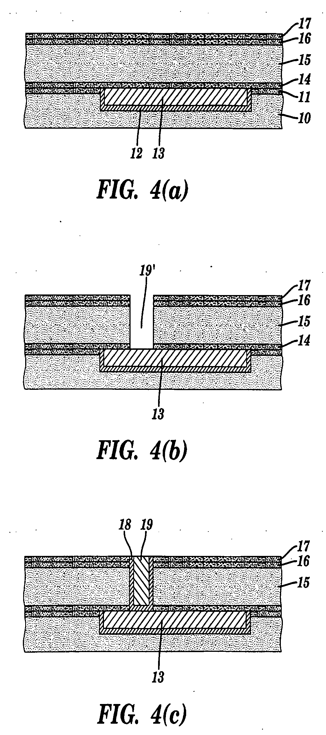
[0023] the invention is shown in FIG. 1, which includes a first dielectric layer 10. At least one first conductor 13 is embedded in the first dielectric layer 10 and has a top surface coplanar with the top surface of layer 10. Optionally, a hardmask layer 11 may be deposited on dielectric layer 10, in which case the conductor 13 has a top surface coplanar with the top surface of hardmask layer 11. A conductive liner 12 is also optionally disposed between conductor 13 and dielectric layer 10.

[0024] A second dielectric layer 15 overlies first dielectric layer 10. Optionally, a cap layer 14 separates second dielectric layer 15 from first dielectric layer 10 and first conductor 13. Second dielectric layer 15 has at least one second conductor embedded therein. The second conductor comprises at least one first portion 19, the via or stud, and at least one second portion 21, the line conductor. The first portion 19 overlies and is in electrical contact with the first conductor 13. The seco...

third embodiment

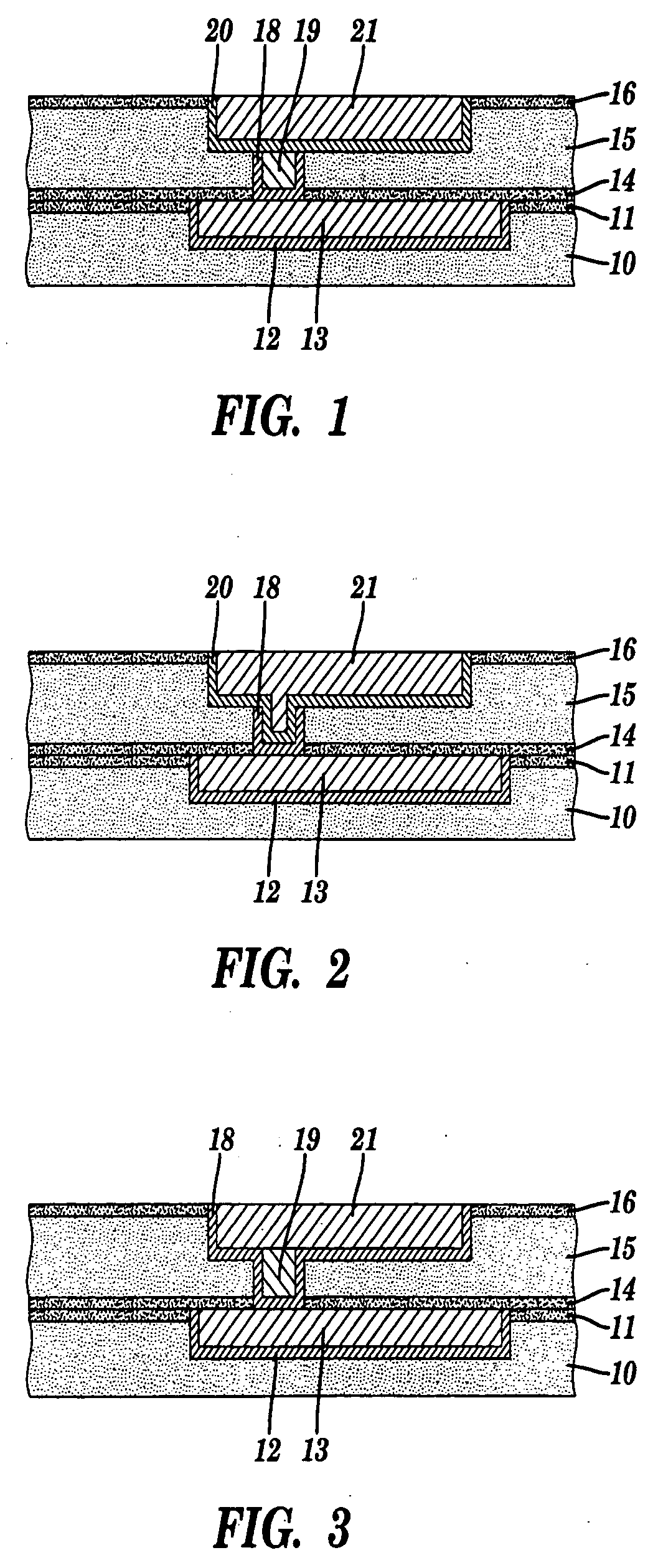
[0030] the invention is shown in FIG. 3, and differs from the embodiment shown in FIG. 1 in that first portion 19 and second portion 21 of the second conductor are both surrounded by liner 18. In other words, first portion 19 and second portion 21 do not have separate liners, as in the embodiment shown in FIG. 1. Rather, a single liner 18 surrounds the bottom and sidewalls of both first portion 19 and second portion 21.

[0031] For the embodiment shown in FIG. 3, the same materials may be used for each of the features discussed with regard to the embodiment shown in FIG. 1. The second portion 21 of the second conductor, i.e. the line conductor, preferably has a total thickness of about 100 to 5000 nm, more preferably about 300 nm. The first portion 19 of the second conductor, i.e. the via, preferably has a height of about 100 to 5000 nm, more preferably about 300 nm. The liner 18 in the via and trench preferably has a thickness of about 2 to 50 nm, more preferably about 20 nm.

[0032] T...


PUM


Abstract

Methods are disclosed for forming dual damascene back-end-of-line (BEOL) interconnect structures using materials for the vias or studs which are different from those used for the line conductors, or using materials for the via liner which are different from those used for the trench liner, or having a via liner thickness different from that of the trench liner. Preferably, a thick refractory metal is used in the vias for improved mechanical strength while using only a thin refractory metal in the trenches to provide low resistance.

Description

BACKGROUND OF INVENTION[0001] This invention relates to the formation of back-end-of-line (BEOL) interconnect structures in integrated circuits. More particularly, this invention relates to new methods of forming dual damascene interconnect structures using materials for the vias or studs which are different from those used for the line conductors.[0002] The semiconductor industry roadmap calls for lowering the dielectric constant on the insulation surrounding multi-level on-chip The dielectric constant must be lowered so as to reduce the parasitic capacitive load to the integrated circuits, as well as to reduce the capacitive coupling between neighboring interconnects.[0003] Reducing dielectric constant often comes with a concomitant reduction in insulator mechanical properties such as modulus, hardness, thermal conductivity and fracture toughness. Significant stresses can develop in the structure due to thermal expansion mismatches with the substrate and the metal interconnects. T...

Claims


Application Information

Patent Timeline
IPC IPC(8): H01L21/768
CPCH01L21/76807H01L21/76808H01L21/76811H01L21/76813H01L21/76843H01L21/76846H01L21/76865H01L2924/0002H01L21/76877H01L23/53238H01L23/53295H01L2924/00H01L21/28H01L21/768
Inventor GAMBINO, JEFFREY P.COONEY, III, EDWARDSTAMPER, ANTHONYMOTSIFF, WILLIAM THOMASLANE, MICHAELSIMON, ANDREW
Owner AURIGA INNOVATIONS INC
Why Eureka
Try Eureka