

Transparent electroconductive film, method for manufacture thereof, and touch panel
a technology of electroconductive film and transparent conductive layer, which is applied in the direction of conductive layers on insulating supports, instruments, other domestic objects, etc., can solve the problems of deterioration in appearance, lowering the electrical properties of touch panels provided with transparent conductive layers, and insufficient durability of touch panels having composite materials
Inactive Publication Date: 2004-12-30
BRIDGESTONE CORP
View PDF23 Cites 144 Cited by
- Summary
- Abstract
- Description
- Claims
- Application Information
AI Technical Summary
Benefits of technology
[0011] The object of the present invention is to provide a touch panel in which the above problems are solved, and in which peeling between a transparent conductive layer and an undercoat layer does not occur and the transparent conductive layer is not damaged even for long-term use to show excellent durability, and further which can be easily prepared, and further to provide a transparent conductive plate usable for preparing the touch panel (a third invention).
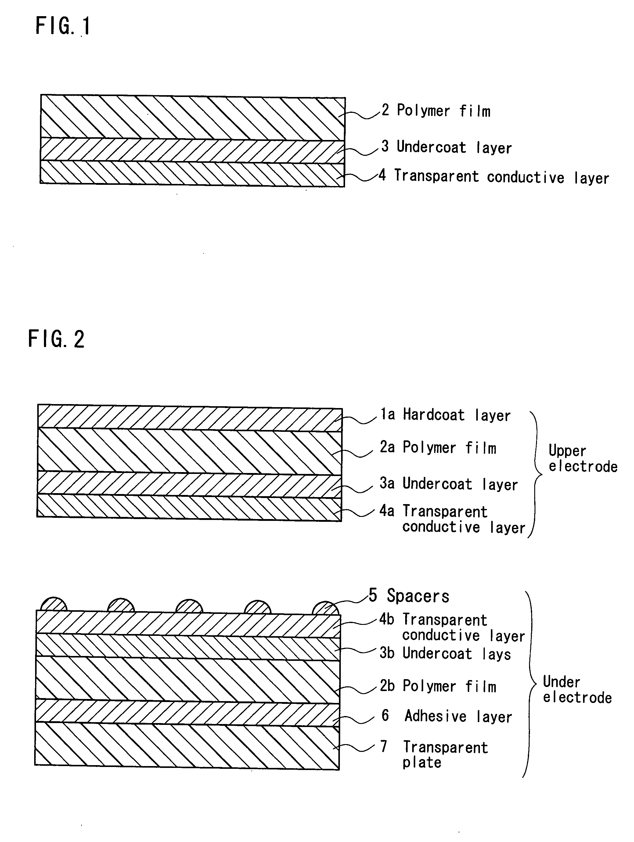
[0080] The sixth invention is provided by a touch panel having excellent mechanical properties and free from falling and peeling of the transparent conductive layer, which has a future that a first transparent conductive layer of an upper electrode is formed from material different from that of a second transparent conductive layer of a lower electrode whereby physical and chemical affinity between the upper and lower electrodes is interrupted.
Problems solved by technology
It has revealed that the undercoat layer described in JA02-66809 does not bring about satisfactory bonding strength between the polymer film and transparent conductive layer and therefore the transparent conductive layer is apt to be exfoliated when it undergoes a durability test by writing.
Hence, a touch panel provided with the transparent conductive layer is lowered in the electrical properties and deteriorated in the appearance.
According to study of the present inventors, however, the touch panel having the composite did not show a sufficient durability.
In more detail, when a surface of an upper electrode prepared using the composite repeatedly undergoes input operation by a pen or fingertip, the transparent electrode generates crack and peeling from the polymer film in course of time.
The damage such as the crack or peeling reduces the electrical properties such as uniformity of electrical resistance values (resistivities), and hence does not bring out the excellent durability.
According to further study of the present inventors, it has been revealed that the damage is frequently caused by insufficient bonding strength between an adhesive layer and a PET (polyethylene terephthalate) film usually employed as a substrate for a composite of substrate / adhesive layer / substrate.
The touch panel provided with the upper and lower electrodes using the same kind of transparent conductive layer described in JA02-66809 does not show excellent durability because resistance to scratching of the transparent conductive layer on the polymer film as the upper electrode is poor.
However, the transparent conductive layer is a polymer film, which is restricted in enhancement of heat resistance.
Further, it is necessary to conduct the heat treatment at 150.degree. C. for a relative long time period to enhance the heat resistance, which results in disadvantage in terms of productivity and cost.
The damage such as the crack or peeling reduces the electrical properties such as uniformity of electrical resistance values, and hence does not bring out the excellent durability.
However, it is difficult to control the resistivity in case the thickness of film is reduced.
Furthermore, as mentioned above, according to study of the present inventors, it has been revealed that the composite prepared by using the adhesive layer described in JA02-66809 shows insufficient durability and therefore occurrence of crack and peeling of the transparent electrode from the polymer film in course of time.
The damage such as the crack or peeling reduces the electrical properties such as uniformity of electrical resistance values, and hence does not bring out the excellent durability.
According to further study of the present inventors, it has been revealed that the damage is frequently caused by insufficient bonding strength between an adhesive layer and a PET (polyethylene terephthalate) film usually employed as a substrate for a composite of substrate / adhesive layer / substrate.
When the film has the thickness of less than 13 .mu.m, the upper electrode having the film does not show sufficient durability.
When the film has the thickness of more than 0.5 mm, the resultant touch panel has increased thickness per se to injure the flexibility.
When the thickness is too large, the transparent conductive layer cannot have enhanced conductivity corresponding to the increase thickness and suffers from increased cost for forming film and increased thickness of the transparent conductive film.
When the thickness is excessively reduced, the protective layer does not sufficiently serve to protect the transparent conductive layer.
When the film has the thickness of less than 13 .mu.m, the upper electrode having the film does not have sufficient durability.
When the film has the thickness of more than 0.5 mm, the resultant touch panel has increased thickness to injure the flexibility.
When the content is less than 20 weight %, the crosslinked density obtained by crosslinking (curing) the copolymer under heating is insufficient.
When the content is more than 80 weight %, the copolymers (I) and (II) show reduced softening temperature whereby the storage comes to difficult to give practical problem while the copolymer (III) shows extremely reduced bonding strength and poor durability.
When the compound is used in an amount of more than 50 weight %, there are some cases where the preparation of a coating liquid for forming the adhesive layer comes to difficult or the coating properties of the liquid becomes poor.
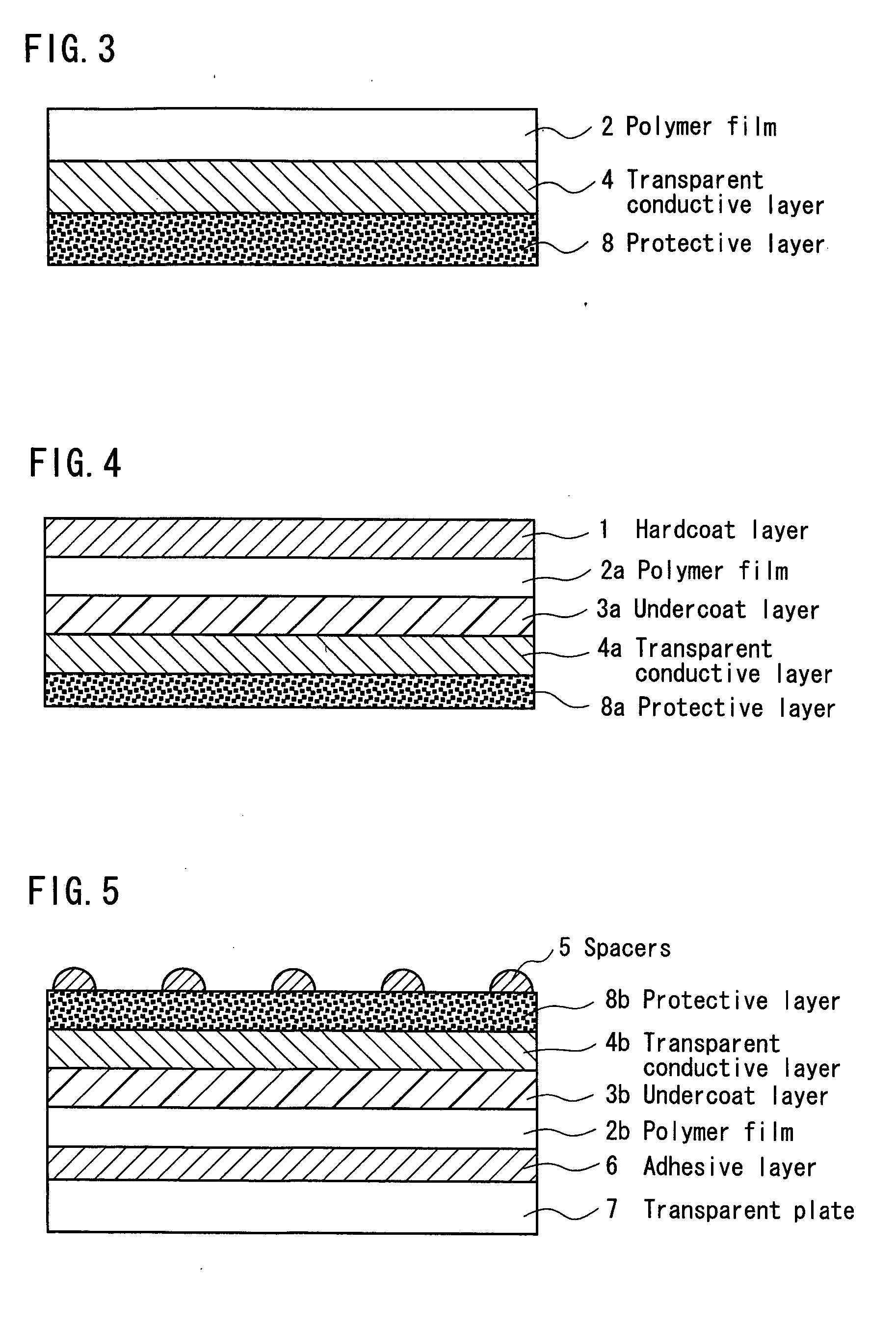
When the thickness of the protective layer is excessively reduced, the protective effect by the formation of the layer cannot be sufficiently obtained.
The excessively increased thickness brings about the reduction of transparency or conductivity, and further the increased thickness of the transparent conductive film.
When the ITO film is excessively thin, the film does not show sufficient conductivity.
When the ITO film is excessively thick, the film show extremely reduced resistivity to bring about a touch panel not having good response.
Further this ITO film is costly prepared and has increased thickness.
When a thickness of the transparent conductive layer, depending upon the materials used therein, is too small, the transparent conductive layer cannot have sufficient conductivity.
When the thickness is too large, the transparent conductive layer cannot have reduced resistivity not to give good response of the resultant touch panel, and suffers from increased cost for forming film and increased thickness of the transparent conductive film.
When the thickness of the adhesive layer 19a, 19b bonding the upper electrode to the lower electrode is excessively thick, the pushing with a pen or fingertip does not bring about turning on electricity because an interval between the upper and lower electrodes is too increased, which makes it impossible to input to the touch panel.
Excessively reduced thickness of the adhesive layer leads to frequent occurrence of input error because a small impact brings about turning on electricity.
Method used
View moreImage
Smart ImageViewing Examples

Examples
example 23
[0384] A touch panel was prepared by using the upper electrode 2 and the lower electrode 1.
Login to View More PUM
| Property | Measurement | Unit |
|---|---|---|
| heat resistance | aaaaa | aaaaa |
| electrical resistance | aaaaa | aaaaa |
| thickness | aaaaa | aaaaa |
Abstract
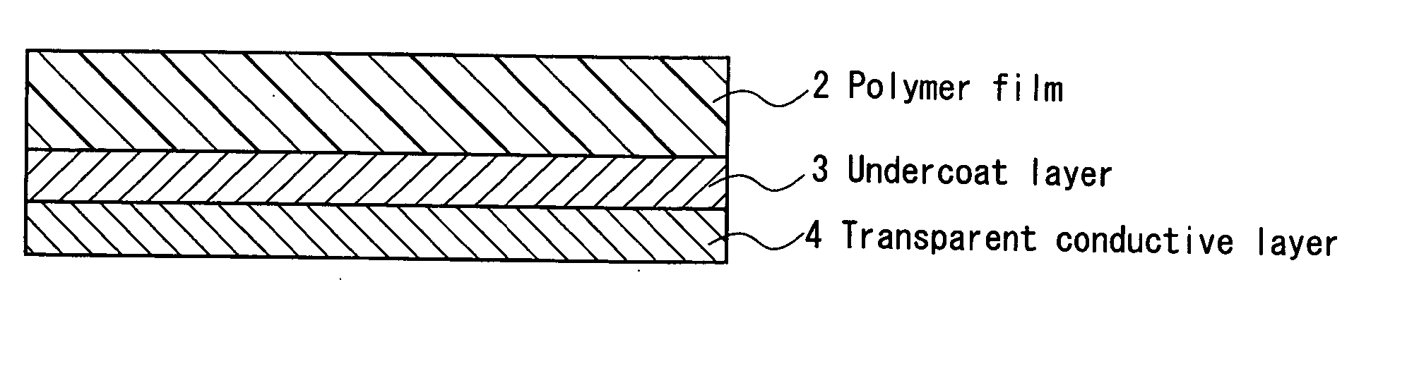
A transparent conductive film comprising a polymer film and a transparent conductive layer provided thereon, especially a transparent conductive film improved in durability and mechanical and electrical properties, a process for the preparation thereof, and a touch panel provided with the transparent conductive film, as well as transparent conductive plate and the process for the preparation thereof. The transparent conductive film comprising a polymer film, an undercoat layer and a transparent conductive layer which are superposed in this order, and the undercoat layer contains a compound having at least one selected from an amino group and a phosphoric acid group.
Description
BACKGROUND OF INVENTION[0001] 1. Field of the Invention[0002] The present invention relates to a transparent conductive film having a polymer film and a transparent conductive layer provided thereon, especially a transparent conductive film improved in durability and mechanical and electrical properties, a process for the preparation thereof, and a touch panel provided with the transparent conductive film, as well as transparent conductive plate and the process for the preparation thereof.[0003] 2. Description of the Related Art[0004] A touch panel according to resistance sensitive system, in which signals are input by pushing a panel with a fingertip or pen and bringing the panel in contact with an opposite electrode to turn on electricity, is advantageous to enable reduction of the size, weight or thickness. Therefore, the touch panel is widely used in input equipments of various home appliances and portable terminals.[0005] The touch panel according to resistance sensitive system...
Claims
Login to View More Application Information
Patent Timeline
 Patent Type & AuthorityApplications(United States)
IPC IPC(8): B29C45/14B32B7/02B32B27/08G06F3/033G06F3/045G06F3/048
CPCB29C45/14311B29C45/14811B29K2715/006B29K2995/0005B29K2995/0026Y10T428/2891B32B27/08G06F3/045G06F2203/04103Y10T428/2878B32B7/02Y10T428/31721Y10T428/31605Y10T428/31663Y10T428/31678Y10T428/31786Y10T428/31699Y10T428/31692Y10T428/31511Y10T428/31681Y10T428/31529Y10T428/31609H01B5/14B32B2310/022B32B2264/102B32B2367/00B32B2457/208B32B2307/202B32B27/36
InventorKOBAYASHI, TAICHIKOTSUBO, HIDEFUMIIWABUCHI, YOSHINORINISHIDA, MITSUHIROKUSANO, YUKIHIROOONO, SHINGOYOSHIKAWA, MASATO
OwnerBRIDGESTONE CORP