Insert molded antenna

a technology of molded antennas and antennas, applied in the direction of resonant antennas, electromagnetic radiation sensing, instruments, etc., can solve the problems of cumbersome and aesthetically undesirable, many electronic units such as hand-held mobile terminals, communication units, etc., and achieve the effect of reducing damage susceptibility, facilitating optimization of antenna geometry and aperture, and improving connectivity

Inactive Publication Date: 2005-01-06
SYMBOL TECH LLC
View PDF9 Cites 80 Cited by
  • Summary
  • Abstract
  • Description
  • Claims
  • Application Information

AI Technical Summary

Benefits of technology

[0014] This subject invention facilitates optimizing antenna geometry and aperture, compared to prior art devices in which such optimization is constrained based on the limited amount of ground plane size. Moreover, electronic devices manufactured by employing insert-molded antenna of the present invention are sized smaller than prior art modules. Also, insert-molding the antenna according to the present invention obviates additional secondary assembly operations, while providing a configuration for the antenna that reduces its damage susceptibility during application in harsh environments.
[0015] In another aspect of the invention an electronic flex circuit piece is insert-molded onto a housing compartment. Such flex piece can be laid on a trough of a molded housing compartment and over molded thereupon. Alternatively, the housing and the flex can be molded in one stage. The wide flex radius provided on the flex piece allows for a range of flexural bending and twisting along the edges of the housing without breakage of the flex piece. As such, the flex member can be aligned and accepted with improved connectivity for subsequent attachment via openings in a circuit board or other components adapted for receiving the housing. This further mitigates rupture of flex components during assembly operation. In addition, a housing fabricated with such flexes facilitates any required sealing and provides improved electrostatic discharge protection for the electronic device.

Problems solved by technology

In particular, many electronic units such as hand hold mobile terminals, communication units, and the like have various assembly costs and are generally susceptible to damage during employment in harsh environments.
Such components, while essential for transmitting and receiving electromagnetic propagable electromagnetic waves, have generally been both cumbersome and aesthetically undesirable.
At the same time, they are typically susceptible to damage when the associated unit is being employed in harsh environments.
While it is essential for effective antenna configurations to assume a dimension proportional to the wavelength of the carrier signal, little progress has taken place in attending to minimization of space occupied by antenna structures and other electronic or mechanical equipments, while simultaneously increasing the overall ruggedness and decreasing assembly costs for the associated electronic unit.
However, such an arrangement is typically susceptible to damage during operation in harsh environments.
For instance, an accidental drop of the unit can relocate the antenna from its static position and affect performance of the unit.
Moreover, in some applications the snap latch features generally required for such assemblies can pose problems.
For example, the snap retention features may require space, and for a unit having closely spaced terminals, the retention geometry can become a problem.
These open passages may be required to become sealed for certain applications, thus increasing associated costs.
Accordingly, while such “integration” results in less obtrusive antenna-laden equipment, such advances have not generally attempted to address the manufacturing and structural needs for an ever increasing trend toward integration and miniaturization of electronics.
Such assembly steps are generally time consuming and expensive in manufacturing.
Because of constant and on going contact with these flex units during assembly operations, the flex units are generally broken during fabrication and are thus susceptible to breakage.
This susceptibility to damage and the associated secondary assembly costs also remains a problem area for other components such as subframes, various electronic circuit boards, display units, interface components, connection terminals, keypads and the like, which are assembled as part of the electronic unit and encased by the plastic housing.

Method used


Image

  • Insert molded antenna
  • Insert molded antenna
  • Insert molded antenna

Examples


Embodiment Construction

[0029] The various aspects of the present invention will now be described with reference to the drawings. The invention provides for an apparatus and method for insert-molding various electronic and mechanical parts as part of a housing of an electrical device. The insert-molded parts can be any component amenable to holding up during various insert-molding process steps. Examples of such insert-molding components can include, various type of antennas, flexural members associated with connections, various input / out put devices such as key pad arrangements, circuit boards and the like.

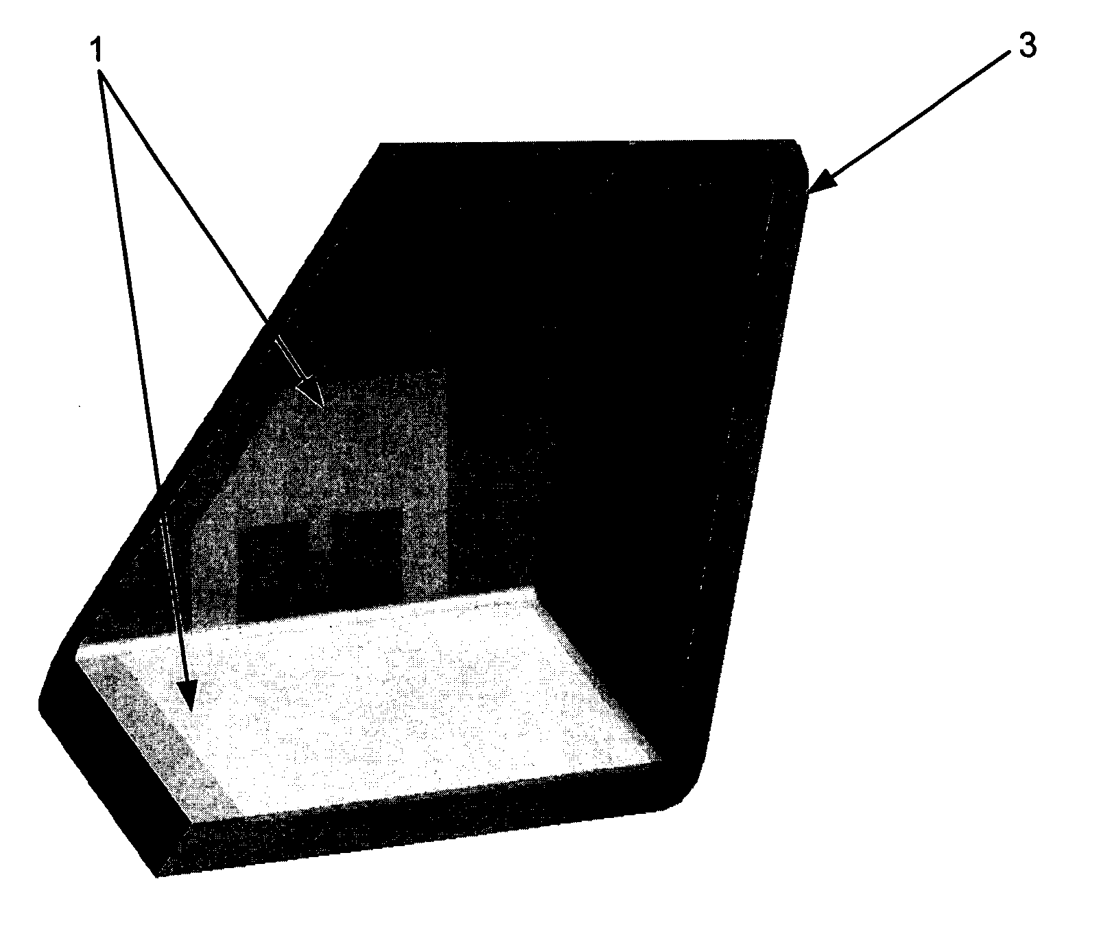
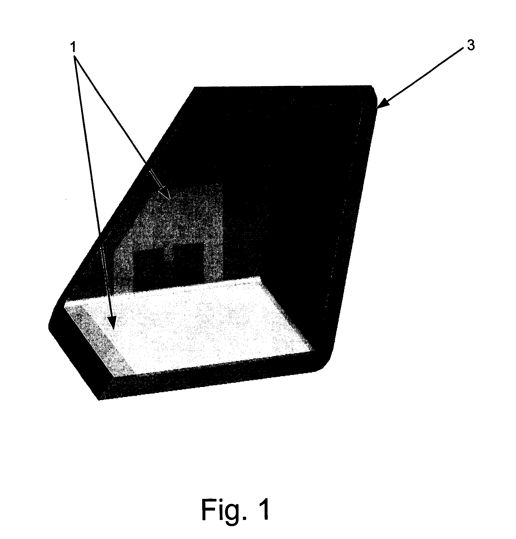
[0030] Referring initially to FIG. 1 a fragmentary perspective view is illustrated that shows an exemplary aspect of the present invention. An antenna 1 is being insert-molded as part of a portion 3 of a housing. The housing can be applied for containment of an electronic device, such as devices employed in numerous types of commercial and industrial applications, (e.g., computers, personal digital ass...


PUM


Abstract

Systems and methods are disclosed for insert-molding various electronic and mechanical parts as part of a housing of an electrical device. The insert molded components can comprise antennas, flex members and circuits, electronic, mechanical, and interface units that have been insert molded as part of a plastic housing that contains the electrical device.

Description

FIELD OF THE INVENTION [0001] The present invention relates to systems and methods of insert-molded components as part of a housing compartment and in particular to electronic and mechanical parts, (e.g. antenna, flex members, electrical components), insert-molded into and / or as part of a plastic housing of an electrical device. BACKGROUND OF THE INVENTION [0002] Typically there is a desire to reduce size of electronic units, while lowering associated assembly costs and improving overall ruggedness. In particular, many electronic units such as hand hold mobile terminals, communication units, and the like have various assembly costs and are generally susceptible to damage during employment in harsh environments. Such units are generally assembled by enclosing internal electrical components, such as a central processing unit (CPU) board, display, keyboard, and internal wiring, within a housing made of plastic or another structural material. The enclosure normally serves as a protectiv...

Claims


Application Information

Patent Timeline
Patent Type & Authority Applications(United States)
IPC IPC(8): H01Q1/24H01Q1/36H01Q1/38H01Q5/00H01Q5/357H01Q5/371
CPCB29C45/14639B29L2031/3456H01Q1/243H01Q5/371H01Q1/38H01Q5/357H01Q1/362
Inventor WULFF, THOMASZANCOLA, RON
Owner SYMBOL TECH LLC
Why Eureka
Try Eureka