
High Power Semiconductor Laser Diode

a laser diode, high-power technology, applied in the direction of lasers, laser details, electrical equipment, etc., can solve the problems of increasing the failure rate at high optical output power, increasing the manufacturing complexity and consequently the price of products, and reducing the size of such a novel laser diode. , the effect of increasing the power outpu

Active Publication Date: 2008-11-06
II VI DELAWARE INC
View PDF14 Cites 32 Cited by
  • Summary
  • Abstract
  • Description
  • Claims
  • Application Information

AI Technical Summary

Benefits of technology

[0014]The result is a very high power laser diode with a reduced susceptibility to failure, in particular by substantially eliminating any current density in the separate section of the ridge waveguide adjacent to the end facet, due to current injection through the electrode on the main ridge section, thus displaying increased reliability compared with prior art devices. The increased device reliability is due to the novel “separate ridge section” design, which differs significantly from the known unpumped end section design.
[0015]Whilst the physical separator is preferably a trench empty of solid material, the entire ridge, including the trench, may be overgrown by solid material in the case where the device is a buried ridge device. Alternatively passivation material may be grown in the trench. The key feature is that the physical separator provides a refractive index contrast, and, although the greatest contrast would be provided by a semiconductor-air boundary, the use in the physical separator of a dissimilar overgrowth material may still provide a sufficient though reduced contrast.
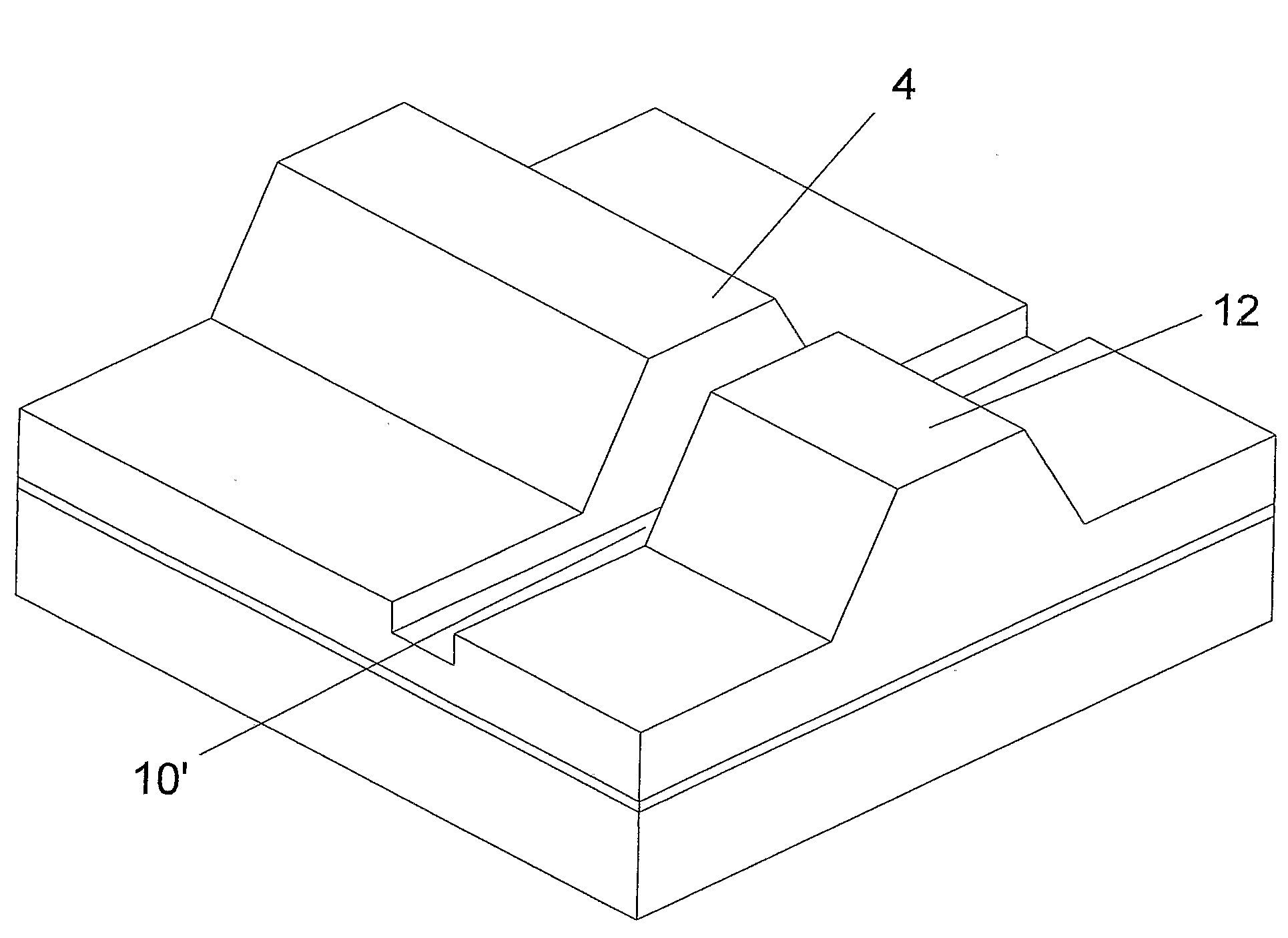
[0016]In an embodiment of the present invention a trench or gap is etched across the width of the laser's ridge, either as part of the ridge etch process, or as a separate etch step, resulting in a passive ridge waveguide end section, i.e. an end section into which substantially no current can diffuse. The result, as mentioned above, is a pump laser chip with minor impact on the electro-optical performance, but with highly improved reliability.
[0017]Ideally substantially no current spreads into the main body of the device, but in practice the current may simply be reduced to a low level. Without the trench, if the control electrode simply stopped short of the facet, the current density profile along the ridge would tail off adjacent to the facet, but to a lesser extent than would be the case if such a trench were provided. Preferably the trench cuts through the top contact layer of highly doped semiconductor material, that is typically present, and into the less conductive, less highly doped region of upper cladding beneath. This cutting through of the contact layer has a disproportionate effect on reducing the current flow into the separate ridge section.
[0018]In addition to the reliability improvement, the separate ridge section may act as a spatial mode filter, i.e. a filter generating higher absorption losses for higher order optical modes. This is due to both the trench and the passive separate ridge section, in the case that the ridge of the end section is narrower than that of the main body of the ridge, and thus reduces the negative impact of non-Gaussian or non-centered light reflected back from the output facet or coupled back into the ridge waveguide, e.g. from a fiber Bragg grating.

Problems solved by technology

One of the major problems of semiconductor laser diodes of the types mentioned above is degradation of the waveguide adjacent to a facet, in particular at the front facet of the laser.
This degradation is believed to be caused by temperature increase at the mirror facet regions, especially at high power outputs, which temperature increase in turn is probably caused by unwanted carrier recombination in these regions and heating due to free carrier injection.
Particularly in the front facet region, an increased failure rate at high optical output powers has been observed.
Such additional processing steps increase the manufacturing complexity and consequently the price of the product.
Further, it appears that the above-identified approaches for reducing the current flow through the end sections of the laser diode's ridge, whether by placing an insulating stripe over the end of the ridge as in U.S. Pat. No. 6,782,024 or by patterning an electrode such that it does not extend over the end section close to the facet as in U.S. Pat. No. 6,373,875 or U.S. Pat. No. 5,844,931, above, do not completely prevent current from spreading into the end sections.

Method used


Image

  • High Power Semiconductor Laser Diode
  • High Power Semiconductor Laser Diode
  • High Power Semiconductor Laser Diode

Examples


Embodiment Construction

[0025]In the following, several embodiments of the invention shall be described by way of example only and by reference to the drawings, which illustrate in:

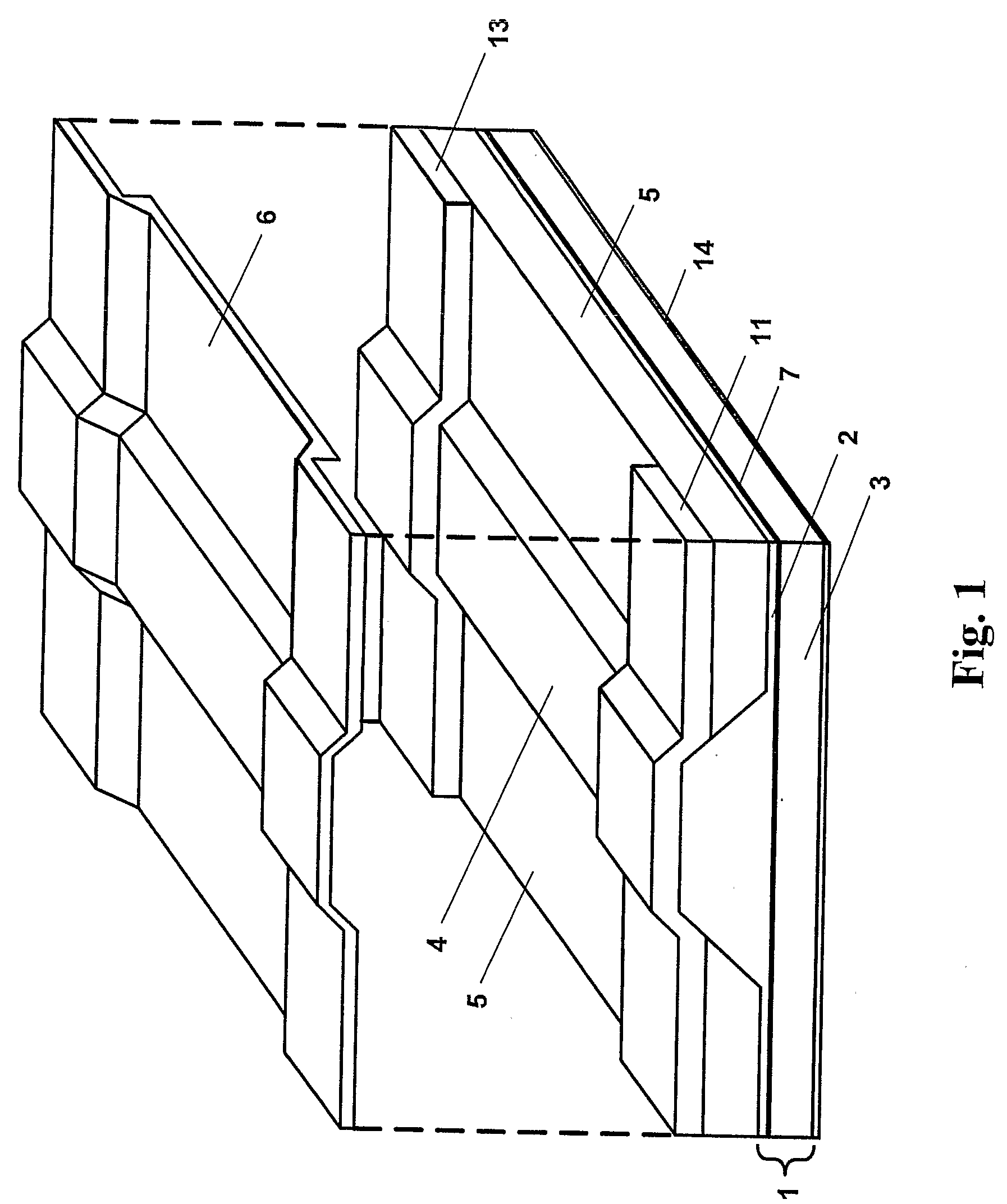
[0026]FIG. 1 a schematic, perspective, “exploded” view of the structure of a prior art ridge waveguide laser diode;

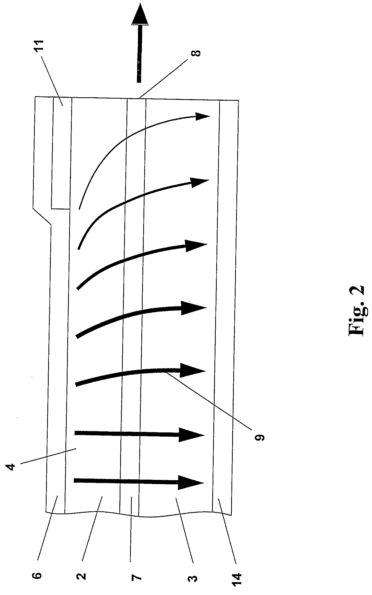
[0027]FIG. 2 the current distribution in a schematic cross section of a prior art ridge waveguide laser diode, adjacent to the front facet;

[0028]FIG. 3 the current distribution in a schematic cross section of a ridge waveguide laser diode according to the present invention, adjacent to the front facet;

[0029]FIGS. 4a-4h schematic, perspective views of several laser diodes according to the present invention;

[0030]FIGS. 5a, 5b a schematic plan view of the use of the invention in a specific design of a cleaved laser;

[0031]FIG. 6 a graph showing simulated losses for the zero order mode and the first order mode of a laser diode according to the invention; and

[0032]FIG. 7 a graph comparing failures of a prior art laser dio...


PUM


Abstract

Semiconductor laser diodes, particularly high power AlGaAs-based ridge-waveguide laser diodes, are often used in opto-electronics as so-called pump lasers for fiber amplifiers in optical communication lines. To provide the desired high power output and stability of such a laser diode and avoid degradation during use, the present invention concerns an improved design of such a device, the improvement in particular significantly minimizing or avoiding (front) end section degradation of such a laser diode and significantly increasing long-term stability. This is achieved by separating the waveguide ridge into an active main ridge section (4) and at least one separate section (12) located at an end of the laser diode, which may be passive. The separation is provided by a trench or gap (10) in the waveguide ridge. The active waveguide section (4) is at least partly covered by the electrode (6) providing the carriers that does not extend to cover the separate ridge section (12), which thus remains essentially free of carriers injected through said electrode (6). There may be a plurality such separate ridge sections, e.g. two separate ridge sections (12, 212), one at each end of the laser diode, dividing the ridge waveguide into three ridge sections, an active main ridge section (4) in the center and a passive separate ridge section (12, 212) at either end. The trenches (10, 110) between the sections and / or the shape and size of the separate ridge section (s) (12, 212) may be adjusted to act as spatial mode filters.

Description

FIELD OF THE INVENTION[0001]The present invention relates to semiconductor laser diodes, particularly to AlGaAs-based laser diodes of high light output power. Such laser diodes are commonly used in opto-electronics, often as so-called pump lasers for fiber amplifiers in the field of optical communications systems, e.g. for Erbium-doped fiber amplifiers. Specifically ridge waveguide laser diodes are suited to provide the desired narrow-bandwidth optical radiation with a stable light output power in a given frequency band. Output power and stability of such laser diodes are of crucial interest and any degradation during normal use must be avoided. The present invention concerns an improved design of such laser diodes, the improvement in particular significantly minimizing or avoiding, compared to prior art designs, front facet degradation of such laser diodes at high light output powers. The present invention further concerns an improved design of such laser diodes in which substantia...

Claims


Application Information

Patent Timeline
IPC IPC(8): H01S5/22H01S5/10H01S5/16H01S5/323
CPCH01S5/0655H01S5/1014H01S5/1017H01S5/1082H01S5/16H01S5/22H01S5/323H01S5/00
Inventor SCHMIDT, BERTHOLDPAWLIK, SUSANNE
Owner II VI DELAWARE INC
Learn More