Enhancing performance characteristics of organic semiconducting films by improved solution processing

a technology of organic semiconducting films and solution processing, which is applied in the field of polymer-based electronic devices, can solve the problems of high-purity silicon required for their manufacture and high cost, and achieve the effects of increasing the absorbance of annealed films, increasing power output, and increasing absorption

Active Publication Date: 2008-12-25
RGT UNIV OF CALIFORNIA
View PDF35 Cites 61 Cited by
  • Summary
  • Abstract
  • Description
  • Claims
  • Application Information

AI Technical Summary

Benefits of technology

[0125]FIG. 32 and FIG. 33 show the effect of additives on maximum peak absorbance values and absorption values at 600 nm, respectively. Films for optical transmission were spun on glass substrates. The various additives generally increase absorbance of the non-annealed films relative to control (non-additive processed film); some additives also increase absorbance of the annealed films relative to control. The increase in absorption can lead to increased power output per unit input of solar light.

Problems solved by technology

The most common type of photovoltaic cell is made from silicon; however, preparing the high-purity silicon required for their manufacture is costly both in economic terms and the energy input required to purify the silicon.

Method used


Image

  • Enhancing performance characteristics of organic semiconducting films by improved solution processing
  • Enhancing performance characteristics of organic semiconducting films by improved solution processing
  • Enhancing performance characteristics of organic semiconducting films by improved solution processing

Examples


example 1

Fabrication and Evaluation of Cells

[0102]PCBM was synthesized as described in the literature (J. C. Hummelen, B. W. Knight, F. LePeq, F. Wudl, J. Org. Chem. 1995, 60, 532), P3HT was purchased from Rieke metals, Baytron P was purchased from H. C. Starck, and all other chemicals were purchased from Sigma / Aldrich and were used as received. Glass slides coated with indium tin oxide were rinsed with soap and water and sonicated once in soapy water, three times in deionized water, and once in each of isopropyl alcohol and acetone for ten minutes prior to being dusted with a nitrogen gun and dried overnight. Prior to spin coating samples were cleaned under UV / Ozone for 30 minutes and dusted again with nitrogen. A layer of Baytron P Poly(ethylene dioxythiophene):Poly(styrene sulfonate) was spin coated at room temperature under atmosphere at 5000 RPM for one minute and then dried at 120° C. for 15 minutes. Devices were then transferred to a glove box which is maintained at less than 5 ppm of...

example 2

Thin Film Transistors

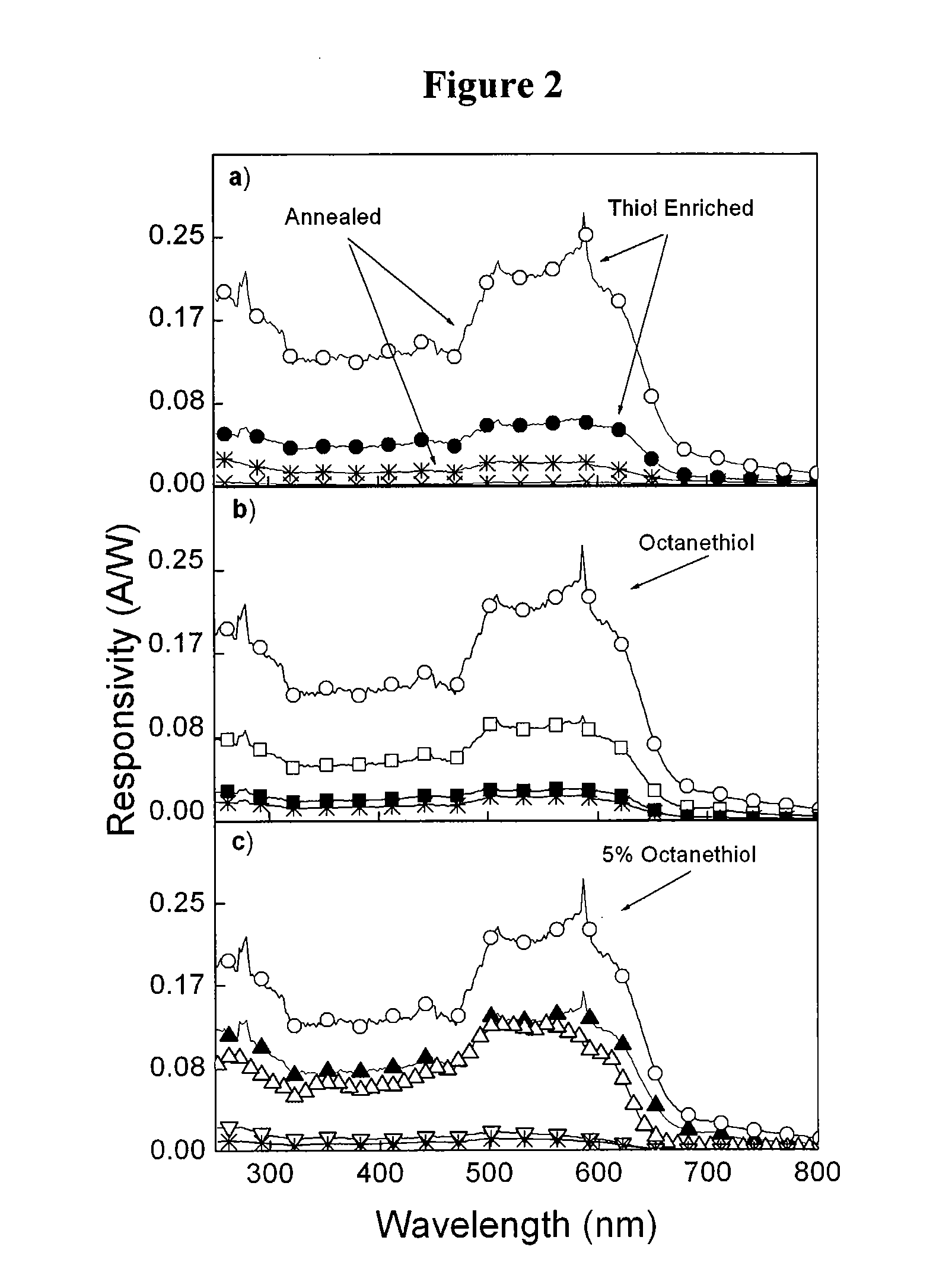
[0118]FIG. 4 shows the behavior of transistors fabricated from semiconductor films (BHJ-NA, dashed lines, and BHJ-5% C8-NA, solid lines). TFT devices were spun at 2000 rpm on heavily doped n-type Si coated with a 200 nm silica dielectric layer treated with octyltrichlorosilane. The source and drain electrodes comprised of 50 nm thick Au deposited on a 5 nm thick Ti adhesion layer in a bottom contact geometry; the TFT channel lengths were 5 or 10 μm and the channel width was 1 mm. Films fabricated with addition of 5% octanethiol show dramatic increases in current at each voltage tested.

example 3

X-Ray Diffraction Results

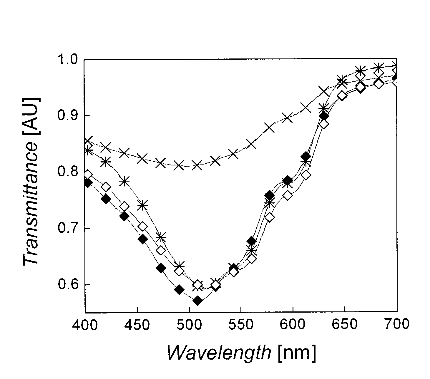
[0119]FIG. 5 and FIG. 30 show the results of X-ray diffraction studies on films processed with and without additive and with or without annealing. Films for X-ray diffraction were spun on glass substrates. Both annealing and use of additive induce significant changes in the X-ray diffraction pattern as compared to the non-annealed film cast without additive, indicative of underlying changes in film structure. FIG. 5 depicts X-ray diffraction results highlighting the diffraction peak for P3HT in P3HT / PCBM films cast from toluene BHJ-NA (x's, X), BHJ-A (asterisks or *, ), BHJ-0.75% C8-NA (filled diamonds, ♦), and BHJ-0.75% C8-A (open diamonds, ⋄). FIG. 30 depicts X-ray diffraction results highlighting the diffraction peak for P3HT in P3HT / C-60 PCBM films cast from chlorobenzene (squares) or chlorobenzene containing 2.5% octanethiol (circles) either before annealing (closed shapes) or after annealing (open shapes). The films are cast using toluene (FIG. 5) a...


PUM

PropertyMeasurementUnit
external quantum efficiencyaaaaaaaaaa
molecular weightaaaaaaaaaa
transparentaaaaaaaaaa

Abstract

Improved processing methods for enhanced properties of conjugated polymer films are disclosed, as well as the enhanced conjugated polymer films produced thereby. Addition of low molecular weight alkyl-containing molecules to solutions used to form conjugated polymer films leads to improved photoconductivity and improvements in other electronic properties. The enhanced conjugated polymer films can be used in a variety of electronic devices, such as solar cells and photodiodes.

Description

CROSS REFERENCE TO RELATED APPLICATIONS[0001]This application claims the priority benefit of U.S. Provisional Patent Application No. 60 / 872,221, filed Dec. 1, 2006, of U.S. Provisional Patent Application No. 60 / 919,602, filed Mar. 23, 2007, and of U.S. Provisional Patent Application No. 60 / 938,433, filed May 16, 2007. The entire contents of those applications are hereby incorporated by reference herein.STATEMENT REGARDING FEDERALLY SPONSORED RESEARCH OR DEVELOPMENT[0002]This invention was made in part during the course of work under grant numbers DE-FG02-06ER46324 and DE-FG24-04NT42277 from the United States Department of Energy, grant number N-00014-04-0411 from the Office of Naval Research of the United States Navy, and under an NDSEG Fellowship from the United States Department of Defense. The United States Government has certain rights in this invention.TECHNICAL FIELD[0003]This application relates to polymer-based electronic devices and particularly to solution processing metho...

Claims


Application Information

Patent Timeline
Patent Type & Authority Applications(United States)
IPC IPC(8): H01L51/00H01L51/40
CPCB82Y10/00H01L51/0007H01L51/0028H01L51/0036H01L51/0047H01L51/4253H01L31/0256H01L51/005Y02E10/549H10K71/15H10K71/441H10K85/113H10K85/215H10K30/30H10K85/60
Inventor BAZAN, GUILLERMO C.HEEGER, ALAN J.MOSES, DANIELPEET, JEFFREY
Owner RGT UNIV OF CALIFORNIA
Why Eureka
Try Eureka