Low cost electromagnetic energy absorbers manufactured from conductive loaded resin-based materials

a technology of electromagnetic energy absorbers and loaded materials, which is applied in the direction of resonant antennas, packaging, coupling device connections, etc., can solve the problems of electromagnetic energy becoming unwanted, electromagnetic energy is typically stray, and electromagnetic energy is typically emitted by normal operating electronic devices, and achieves the effect of effective electromagnetic energy absorbers

Inactive Publication Date: 2005-01-06
INTEGRAL TECHNOLOGY INC
View PDF13 Cites 42 Cited by
  • Summary
  • Abstract
  • Description
  • Claims
  • Application Information

AI Technical Summary

Problems solved by technology

A normally operating electronic device will typically emit significant amounts of stray electromagnetic energy due electrical charge accelerations occurring in the device.
That is, the electromagnetic energy becomes an unwanted, interference signal in the second device.
Further, natural sources, such as the sun, generate electromagnetic energy that can create signal interference in the proposed device.
It is not sufficient to simply ‘bullet proof’ the proposed design from outside interference.
This type of radar tracking system may be adversely affected by interactions between the transmitted radar energy and structures on the ship such as masts, towers, artillery tubes, and the like.
As a result, significant degradation in tracking ability may occur.

Method used


Image

  • Low cost electromagnetic energy absorbers manufactured from conductive loaded resin-based materials
  • Low cost electromagnetic energy absorbers manufactured from conductive loaded resin-based materials
  • Low cost electromagnetic energy absorbers manufactured from conductive loaded resin-based materials

Examples


embodiment 10

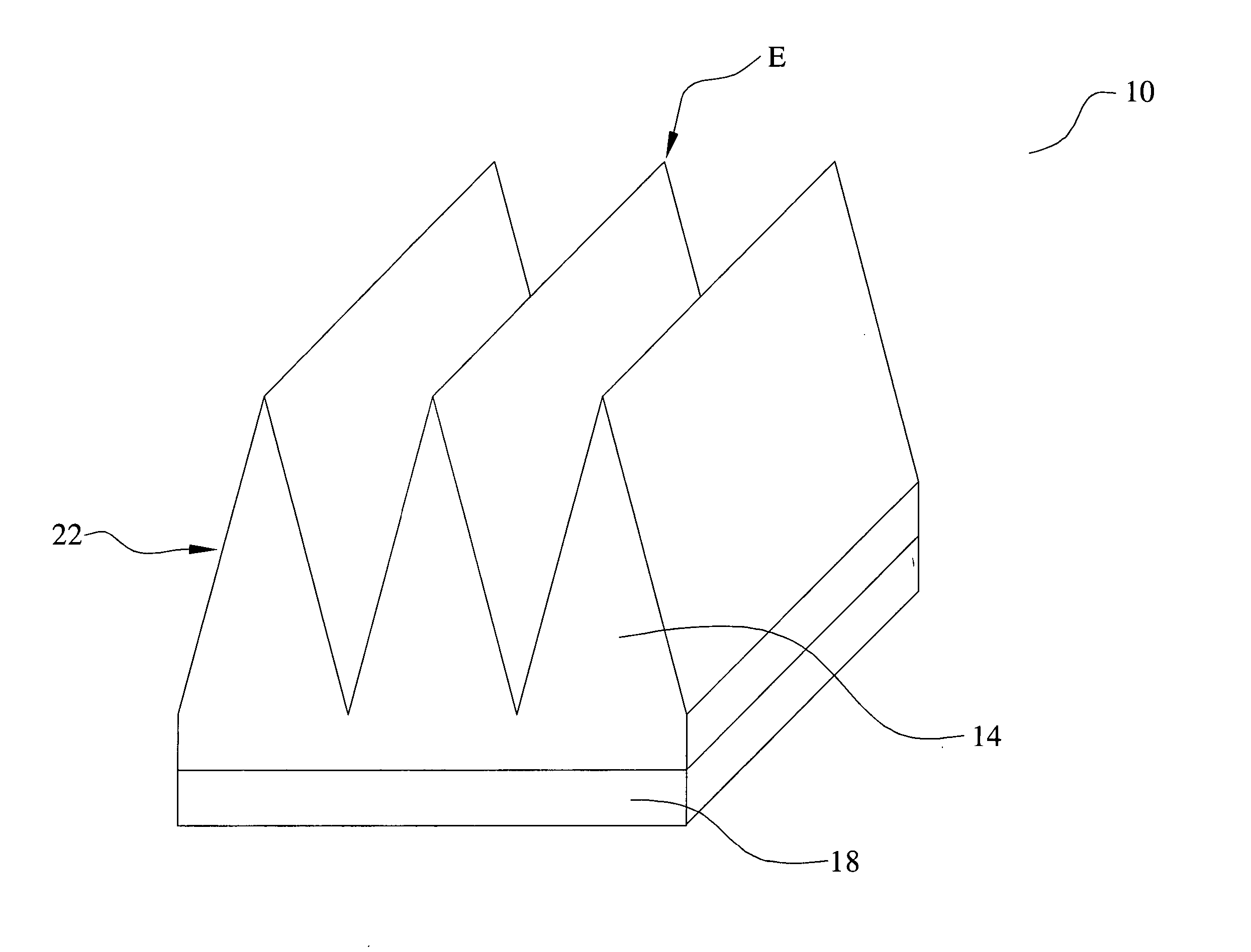
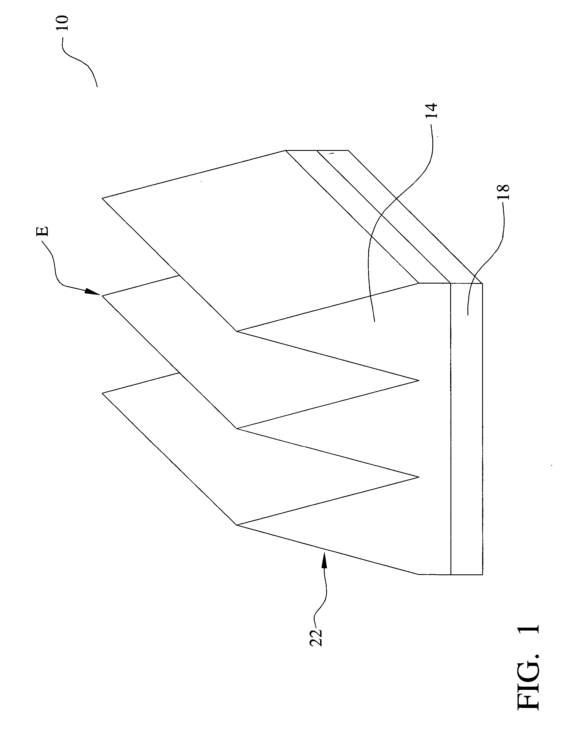
[0050] Referring now to FIG. 1, a first preferred embodiment 10 of the present invention is illustrated. Several important features of the present invention are shown and discussed below. In this embodiment, a pyramidal shaped absorber 14 is formed of the conductive loaded resin-based material of the present invention. This type of absorbing structure is particularly useful in anechoic testing chambers to absorb high level electromagnetic energy and to convert this energy to heat.

[0051] The apexes of the pyramids are oriented toward the energy source (E). Incident energy waves encounter a graded dielectric, because of the shape 22 of the absorber 14, such that the impedance gradually tapers from that of free space to that of the absorber 14. Further, the absorber 14 has a high dielectric content that creates a lossy media for transport of the electromagnetic energy. The smooth transition from free space (air) to absorber space 14 results in little reflection of the incident energy. ...

embodiment 100

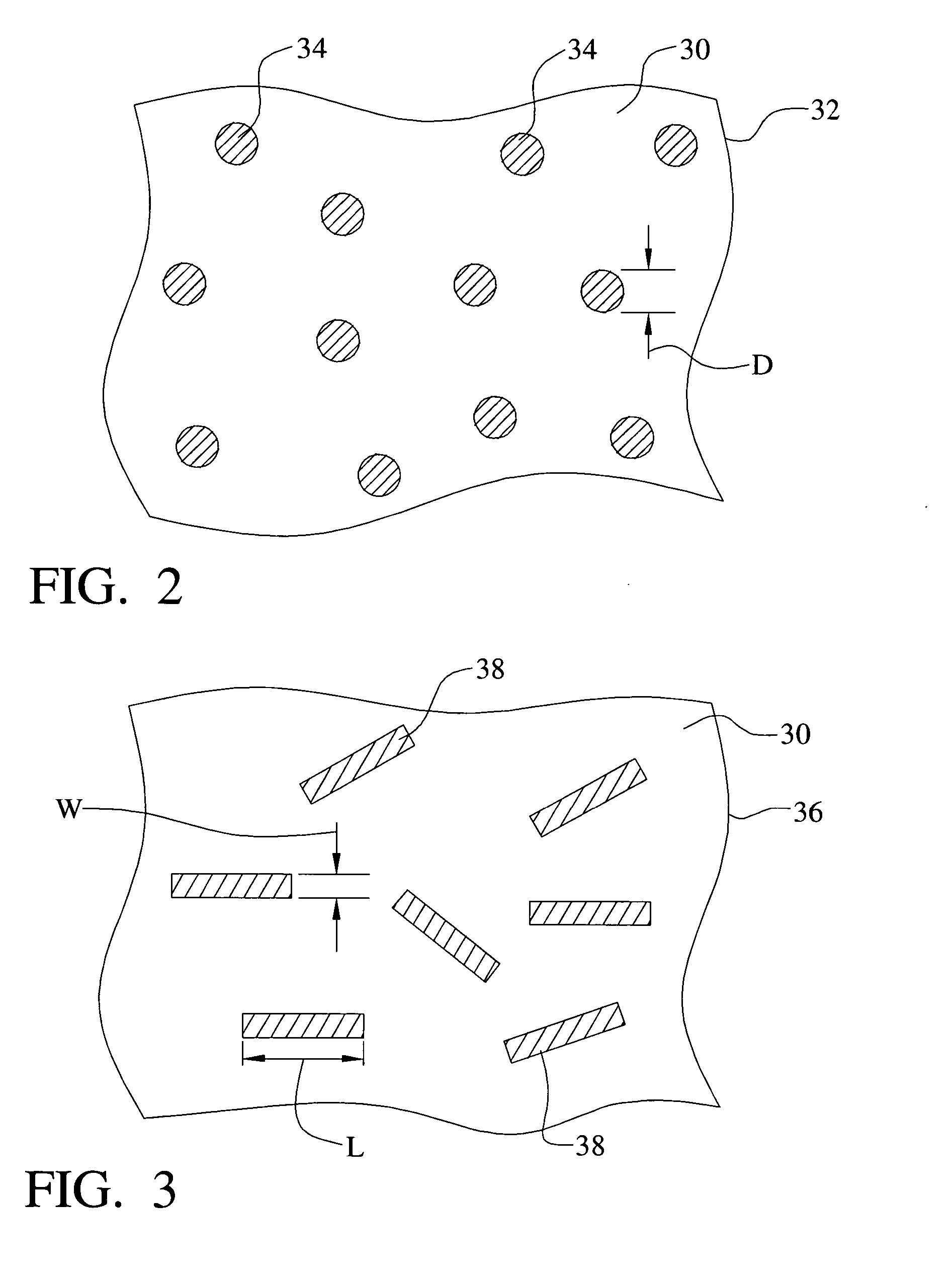
[0053] Referring now to FIG. 7, a second preferred embodiment 100 of the present invention is illustrated. Electromagnetic energy absorbing tiles 104 comprising a conductive loaded resin-based material are shown. In the prior art, magnetic energy absorbing tiles typically comprise a ferrite material. This material interacts with the magnetic field of the electromagnetic energy to convert this energy into heat. In the present invention, the conductive loaded resin-based material of the tiles 104 is formulated with a loading, such as iron, that will interact with the incident magnetic field and convert the energy to heat. In anther embodiment of the present invention, the tiles 104 comprise a non-magnetic conductive loading material.

embodiment 120

[0054] Referring now to FIG. 8, a third preferred embodiment 120 of the present invention is illustrated. Combined, pyramidal and tiled electromagnetic energy absorbers comprising a conductive loaded resin-based material are shown. These absorbers 120 comprise a pyramid structure 124, a tile structure 132, and a backplane structure 128. In one embodiment, the graded dielectric, pyramid shaped absorber 124 comprises a conductive loaded resin-based material as defined in the present invention. In another embodiment, the pyramid structure 124 comprises a non-foamed resin-based material. In another embodiment, the pyramid structure 124 comprises a foamed resin-based material. In another embodiment, the pyramid structure 124 comprises a resin-based material that is covered with a thin layer, or sheet, not shown, of conductive loaded resin-based material. Further, in that embodiment, it is preferred that the inner region 124 comprise a foamed resin-based material.

[0055] In one embodiment ...


PUM

PropertyMeasurementUnit
diameteraaaaaaaaaa
diameteraaaaaaaaaa
lengthaaaaaaaaaa

Abstract

Electromagnetic energy absorbing devices are formed of a conductive loaded resin-based material. The conductive loaded resin-based material comprises micron conductive powder(s), conductive fiber(s), or a combination of conductive powder and conductive fibers in a base resin host. The ratio of the weight of the conductive powder(s), conductive fiber(s), or a combination of conductive powder and conductive fibers to the weight of the base resin host is between about 0.20 and 0.40. The micron conductive powders are formed from non-metals, such as carbon, graphite, that may also be metallic plated, or the like, or from metals such as stainless steel, nickel, copper, silver, that may also be metallic plated, or the like, or from a combination of non-metal, plated, or in combination with, metal powders. The micron conductor fibers preferably are of nickel plated carbon fiber, stainless steel fiber, copper fiber, silver fiber, or the like.

Description

[0001] This Patent Application claims priority to the U.S. Provisional Patent Application 60 / 484,448 filed on Jul. 2, 2003, which is herein incorporated by reference in its entirety. [0002] This Patent Application is a Continuation-in-Part of INT01-002CIP, filed as U.S. patent application Ser. No. 10 / 309,429, filed on Dec. 4, 2002, also incorporated by reference in its entirety, which is a Continuation-in-Part application of docket number INT01-002, filed as U.S. patent application Ser. No. 10 / 075,778, filed on Feb. 14, 2002, which claimed priority to U.S. Provisional Patent Applications Ser. No. 60 / 317,808, filed on Sep. 7, 2001, Ser. No. 60 / 269,414, filed on Feb. 16, 2001, and Ser. No. 60 / 268,822, filed on Feb. 15, 2001.BACKGROUND OF THE INVENTION [0003] (1) Field of the Invention [0004] This invention relates to electromagnetic energy absorbers and, more particularly, to electromagnetic energy absorbers molded of conductive loaded resin-based materials comprising micron conductiv...

Claims


Application Information

Patent Timeline
Patent Type & Authority Applications(United States)
IPC IPC(8): B29C45/00B29C70/58B29C70/88G06K19/077H01Q1/12H01Q1/24H01Q1/32H01Q1/36H01Q1/38H01Q1/40H01Q9/04H01Q9/16H01Q9/30H01Q17/00H01Q21/00H01R13/658H05K1/09H05K3/10
CPCB29K2995/0005Y10T428/1328B29C70/58B29C70/882B29C45/0001B29C45/0013G06K19/07749H01Q1/243H01Q17/00H05K1/095H05K3/101H05K3/107H05K2201/0281H05K2201/09118H05K2203/0113H01R13/6599B29L2031/3456Y10T428/249972
Inventor AISENBREY, THOMAS
Owner INTEGRAL TECHNOLOGY INC
Why Eureka
Try Eureka