Method of stabilizing parasitic capacitance in an LCD device

a parasitic capacitance and liquid crystal display technology, applied in non-linear optics, instruments, optics, etc., can solve the problems of serious affecting display quality, method is still subject to misalignment problems, and conventional lcd process has several problems, so as to achieve stable parasitic capacitance in lcds and improve display quality

Inactive Publication Date: 2005-01-06
AU OPTRONICS CORP
View PDF12 Cites 7 Cited by
  • Summary
  • Abstract
  • Description
  • Claims
  • Application Information

AI Technical Summary

Benefits of technology

[0015] The present invention improves on the prior art in that the data lines and the metallic light shield layers are defined on the first silicon oxide layer in the same photolithography procedure. Thus, there is a constant distance between the metallic light shield layer and the data line in each pixel cell. Moreover, the metallic light shield layer can electri

Problems solved by technology

Nevertheless, the conventional LCD process has several problems.
The unsettled parasitic capacitance seriously affects di

Method used


Image

  • Method of stabilizing parasitic capacitance in an LCD device
  • Method of stabilizing parasitic capacitance in an LCD device
  • Method of stabilizing parasitic capacitance in an LCD device

Examples


Embodiment Construction

[0021] Reference will now be made in detail to the present preferred embodiments of the invention, examples of which are illustrated in the accompanying drawings.

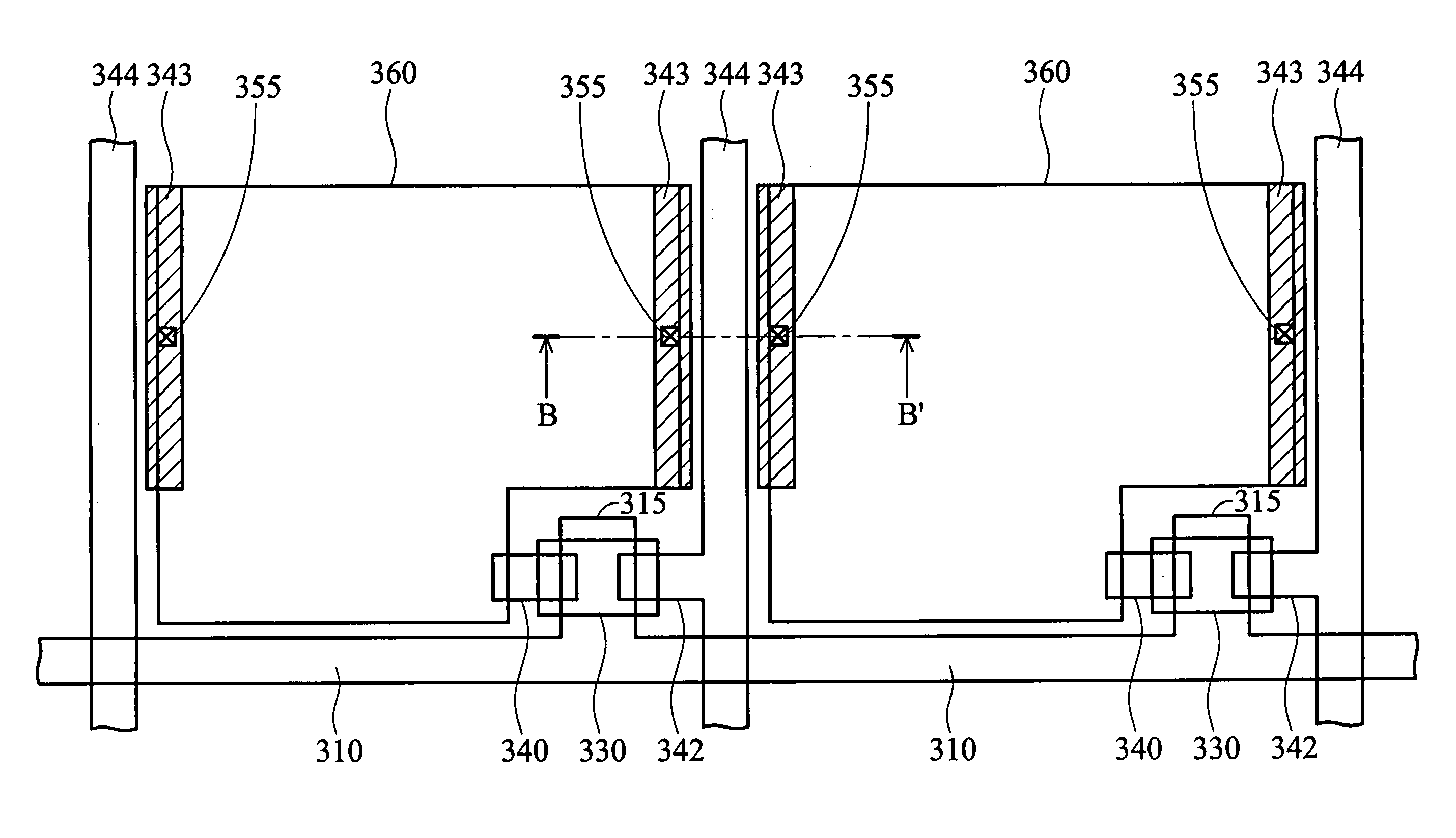
[0022]FIG. 3 is a plan view of an LCD device of the present invention. FIG. 4 is a sectional view taken along line B-B′ of FIG. 3. In order to simplify the illustration, FIG. 3 shows a substrate in two adjacent pixel regions. That is, there may be a large number of pixel regions.

[0023] In FIGS. 3 and 4, a first substrate 300 serving as a lower substrate is provided. The first substrate 300 can be a heat-resistant glass substrate. By performing a photolithography (or patterning) procedure using a first photomask (or reticle), a plurality of transversely expanding gate lines 310 are formed on the first substrate 300. The gate line 310 has a protruding portion 315 serving as a gate 315. Then, a first insulating layer 320 is formed over the first substrate 300 and the gate line 310. The first insulating layer 320 can be a sil...


PUM


Abstract

A method of stabilizing parasitic capacitance in an LCD device. Pluralities of transversely expanding gate lines are formed on a substrate. A first insulating layer is formed on the substrate and the gate lines. By performing a photolithography procedure using a photomask, a plurality of longitudinally expanding data lines and a plurality of metallic light shield layers are formed on part of the first insulating layer, wherein the metallic light shield layers are located on both sides of the data line. A second insulating layer is formed on the metallic light shield layers and the data lines. Transparent conductive layers are formed on part of the second insulating layer. Moreover, conductive plugs penetrating the second insulating layer are formed to electrically connect the metallic light shield layers and the transparent conductive layers.

Description

BACKGROUND OF THE INVENTION [0001] 1. Field of the Invention [0002] The present invention relates to a method of forming a liquid crystal display (LCD) device, and more particularly, to a method of forming an LCD device which stabilizes parasitic capacitance caused by light shield film. [0003] 2. Description of the Related Art [0004] Liquid crystal display (LCD) devices are widely used as displays in devices, such as portable televisions and notebook computers. The LCD device includes a plurality of pixel cells, each including a switching thin film transistor (TFT). In order to improve display quality, striped type light shield layers are usually formed around each pixel cell. Typically, the light shield layers are composed of metal. [0005]FIG. 1 is a partial plane view of a conventional LCD device, showing light shield films formed around each pixel cell. FIG. 2 is a sectional view taken along line A-A′ of FIG. 1. [0006] In FIGS. 1 and 2, by performing a first photolithography proc...

Claims


Application Information

Patent Timeline
IPC IPC(8): G02F1/136G02F1/1362
CPCG02F1/136209G02F1/136286G02F1/13606G02F1/136231
Inventor WU, CHING-HUNGCHEN, RUEI-PEI
Owner AU OPTRONICS CORP
Why Eureka
Try Eureka