Inspection apparatus having two sensors, method for inspecting an object, and a method for manufacturing a photolithography mask

a technology of photolithography mask and inspection apparatus, which is applied in the direction of originals for photomechanical treatment, semiconductor/solid-state device testing/measurement, instruments, etc., can solve the problems of a minimum pin hole defect, a thin film on a residue on a half-tone film or a certain defect, and is difficult to detect with such systems

Active Publication Date: 2005-01-06
KIOXIA CORP
View PDF8 Cites 32 Cited by
  • Summary
  • Abstract
  • Description
  • Claims
  • Application Information

AI Technical Summary

Problems solved by technology

However, certain defects, such as thin film on a residue on a half-tone film or a minimum pin hole defect, are difficult to detect with such systems.
The mask inspection systems described above, however, suffer from various shortcomings, as discussed below.
When combined, the transmitted and reflected images can interfere and cancel the defect signal with one another, thereby creating so-called “dead zones” in the composite image where defects many not be detected.
These systems, however, require complex optics for focusing the transmitted and reflected image optics on to corresponding sensors.
In addition, simultaneous sensing of reflected and transmitted images is further complicated by different optical systems i.e., the transmitted and reflected optics includ...

Method used


Image

  • Inspection apparatus having two sensors, method for inspecting an object, and a method for manufacturing a photolithography mask
  • Inspection apparatus having two sensors, method for inspecting an object, and a method for manufacturing a photolithography mask
  • Inspection apparatus having two sensors, method for inspecting an object, and a method for manufacturing a photolithography mask

Examples


first embodiment

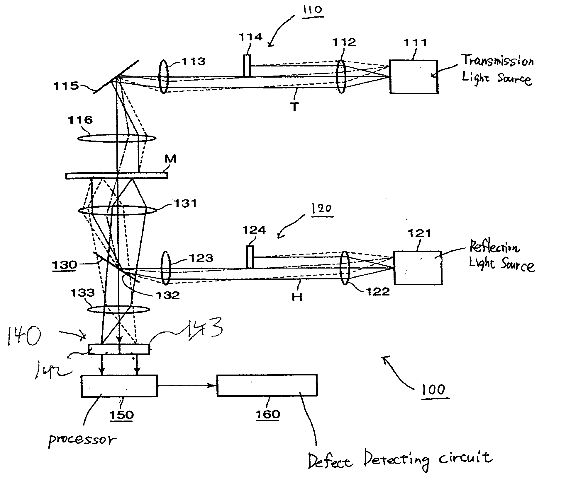
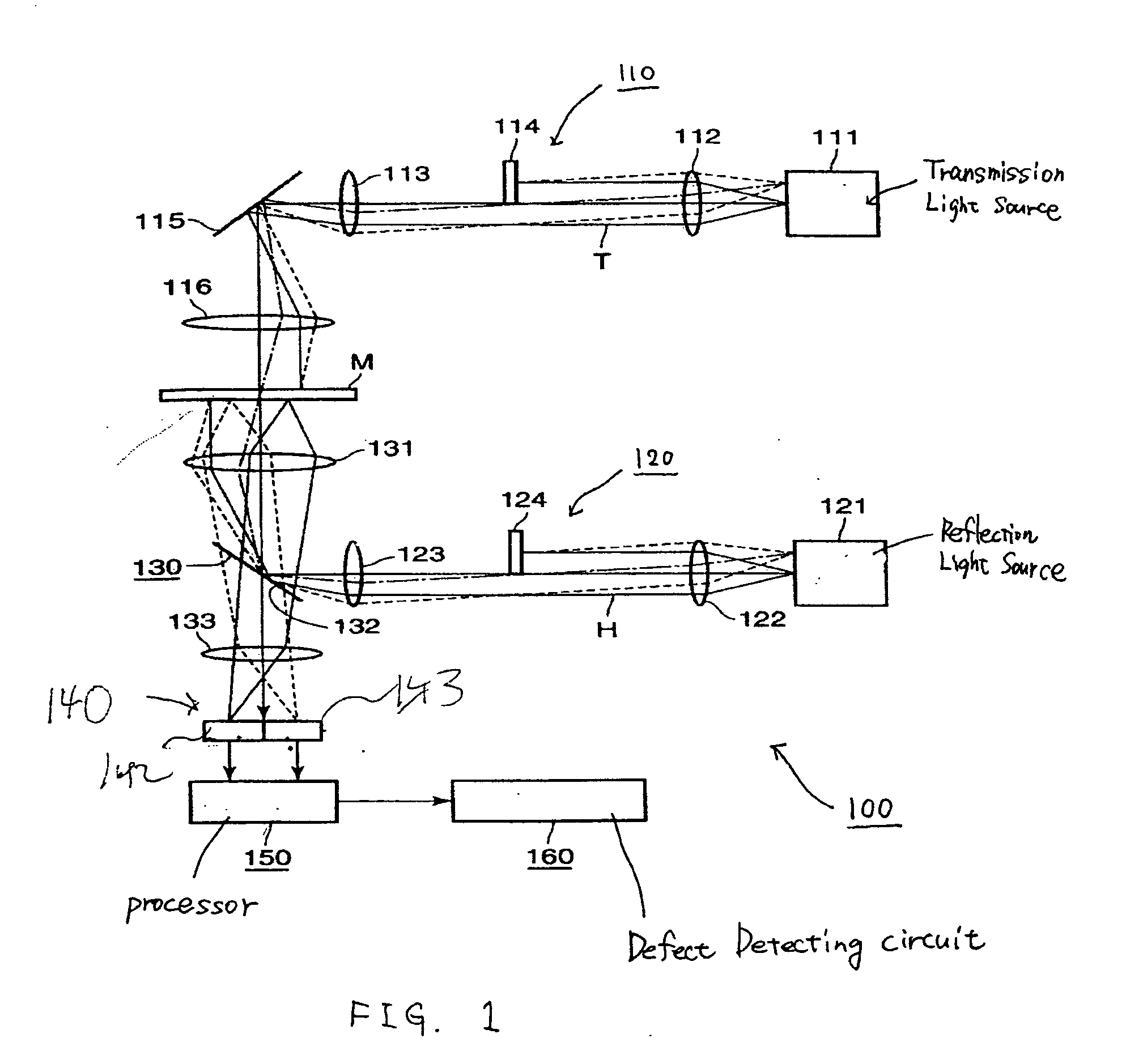
[0068] As discussed above, detection based on both transmitted and reflected images is more accurate than detection based on either image alone. In the first embodiment explained above, imaging optics 130 focuses both a partial transmitted image on first sensor 142 and a partial reflected image on second sensor 143. Accordingly, mask M can be inspected based on detection of both reflected and transmitted images at the same time after sensor output delays image data output from first compensation circuit 152 corresponding to sensor 142, for example. In addition, both reflected and transmitted images are subject to the same distortions and defects of common imaging optics 130, thereby minimizing variations between the images that would otherwise occur if the images were sensed by separate optics. In view of the foregoing, defects can be detected and a high quality mask can be manufactured by inspecting the mask with the apparatus 100 following mask fabrication.

second embodiment

[0069]FIG. 9 illustrates a schematic diagram of a mask inspection apparatus 200 consistent with the present invention. The same reference characters are used to label the same or similar features of in both inspection apparatus 100 and inspection apparatus 200.

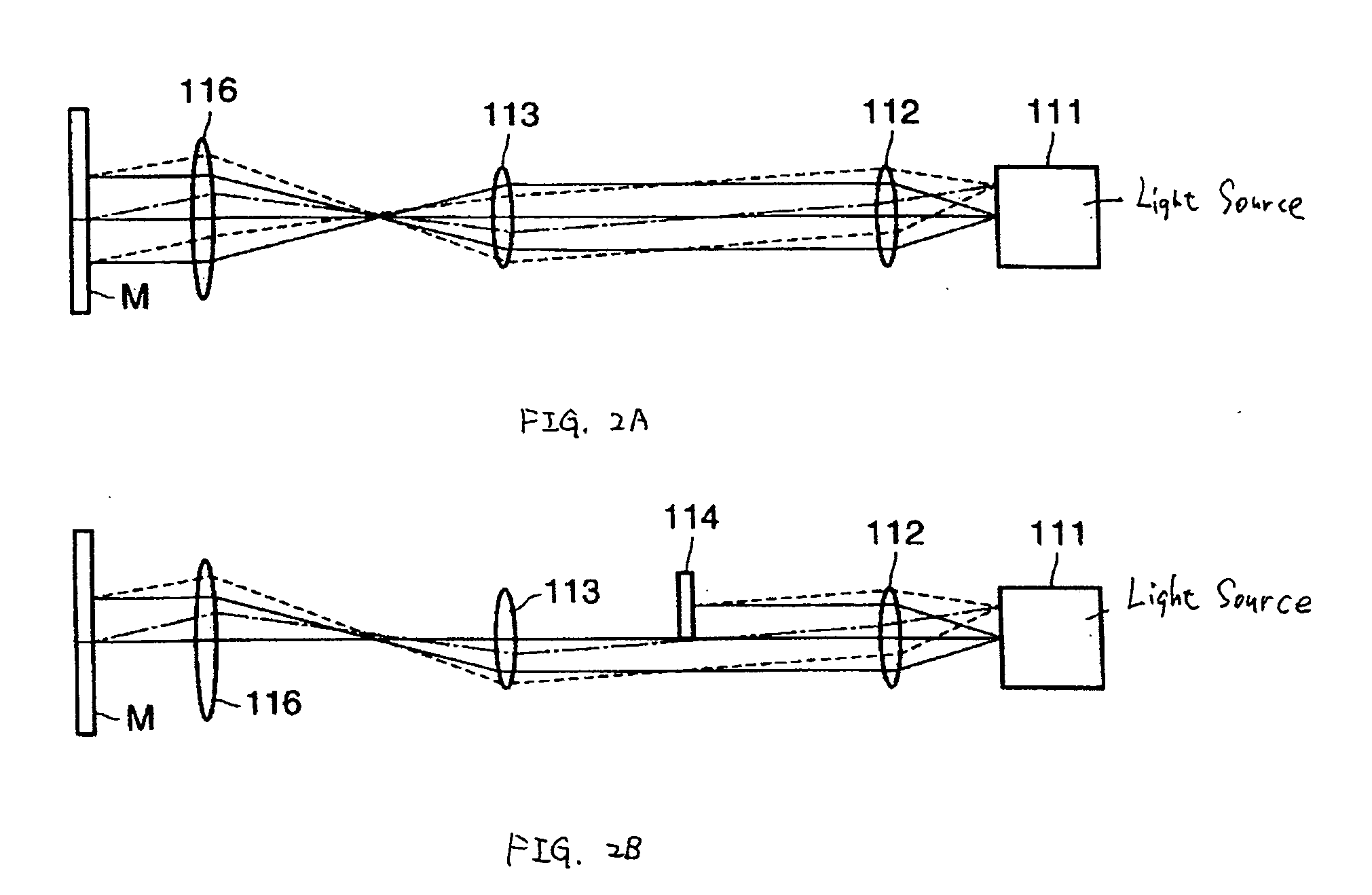
[0070] Mask inspection apparatus 200 is provided with a laser source 201 to expose an object, such as mask M instead of transmission and reflection light sources 111 and 121 shown in FIG. 1. Apparatus 200 also includes a beam expander 202 and a speckles reducing system 203. In addition, apparatus 200 includes an optical system 210 instead of second optical system 120. Further, optical system 210 includes half mirror 211, second aperture 212, a pair of collector lenses 213 and 214, and a mirror 215.

[0071] Half mirror 211 separates a laser beam emitted from light source 201 into laser beams for generating the transmitted and reflected images. Half mirror 132 directs laser beam H toward mask M, after laser beam H passes through ...


PUM


Abstract

A photolithography mask inspection apparatus has at least two sensors. One sensor is configured to sense light transmitted through an object to be inspected, and the other sensor senses light reflected off the object. A first optical system is arranged to expose a first portion of the object with a first light beam, and a second optical system is arranged to expose a second portion of the object, spaced form the first portion, with a second light beam. A third optical system focuses the transmitted light on to the first sensor, as well as the reflected light on to the second sensor. A defect detecting circuit is also provided to detect a defect of the object, based upon image data associated with the reflected and transmitted light.

Description

CROSS REFERENCE TO RELATED APPLICATION [0001] This application is based upon and claims the benefit of priority from prior Japanese Patent Application No. 2003-149336 filed on May 27, 2003, the entire contents of which are incorporated herein by reference. [0002] 1. Field of the Invention [0003] The present invention relates to an inspection apparatus having a first sensor to sense a transmitted image of an object to be inspected and a second sensor to sense a reflected image of the object. The present invention is also directed toward a method for inspecting an object, and a method for manufacturing a mask. [0004] 2. Description of the Related Art [0005] Conventional inspection systems detect defects in an object, such as a semiconductor device or photo-mask (e.g., a photolithography mask) by comparing an image of the object corresponding to light transmitted through the transmitted image of the object with a reference pattern. However, certain defects, such as thin film on a resid...

Claims


Application Information

Patent Timeline
IPC IPC(8): G01N21/956G03F1/84H01L21/66
CPCG01N2021/95676G01N21/956
Inventor INOUE, HIROMUTOJO, TORUNOMURA, TAKEHIKOIMAI, SHINICHI
Owner KIOXIA CORP
Why Eureka
Try Eureka