In-line apparatus and method for manufacturing double-sided stacked multi-chip packages

a technology of integrated circuit chip and packaging method, which is applied in electrical apparatus, semiconductor devices, semiconductor/solid-state device details, etc., can solve the problems of repeated operator intervention, methods and apparatus, and the conventional method of manufacturing multi-chip integrated circuit chip package process is complex, etc., to reduce the amount of handling, simplify the packaging process, and reduce the turn around time.

Active Publication Date: 2005-01-13
SAMSUNG ELECTRONICS CO LTD
View PDF1 Cites 30 Cited by
  • Summary
  • Abstract
  • Description
  • Claims
  • Application Information

AI Technical Summary

Benefits of technology

[0014] The exemplary embodiments of the present invention provide in-line integrated circuit chip packaging apparatuses that can be used to simplify the packaging process and reduce the need for operator involvement during the manufacture of doubled-sided stack multi-chip packages.
[0015] The exemplary embodiments of the present invention also provide methods for manufacturing integrated circuit chip packages that can reduce the associated labor and process times and thereby increase productivity by simplifying the manufacturing process for doubled-sided stack multi-chip packages.
[0030] The in-line integrated circuit chip packaging apparatus according to the exemplary embodiments of the present invention, can simplify the packaging process, reduce the amount of handling by an operator during the packaging operation and reduce the turn around time (TAT), thereby tending to increase the productivity of the integrated circuit chip packaging process.

Problems solved by technology

Therefore, the conventional method of manufacturing multi-chip integrated circuit chip package process is complex, tends to require repeated operator intervention, much of which involves transferring the lead frames of the partially completed devices between various apparatus, and is time-consuming.
The convention methods and apparatus, therefore, tend to decrease productivity.

Method used


Image

  • In-line apparatus and method for manufacturing double-sided stacked multi-chip packages
  • In-line apparatus and method for manufacturing double-sided stacked multi-chip packages
  • In-line apparatus and method for manufacturing double-sided stacked multi-chip packages

Examples


Embodiment Construction

[0043] The present invention will be described more fully with reference to the accompanying drawings, in which exemplary embodiments of the invention are shown. It should be understood, however, that exemplary embodiments of the present invention described herein can be modified in form and detail without departing from the spirit and scope of the invention. Accordingly, the exemplary embodiments described herein are provided by way of example and not of limitation, and the scope of the present invention is not restricted to the particular embodiments described herein.

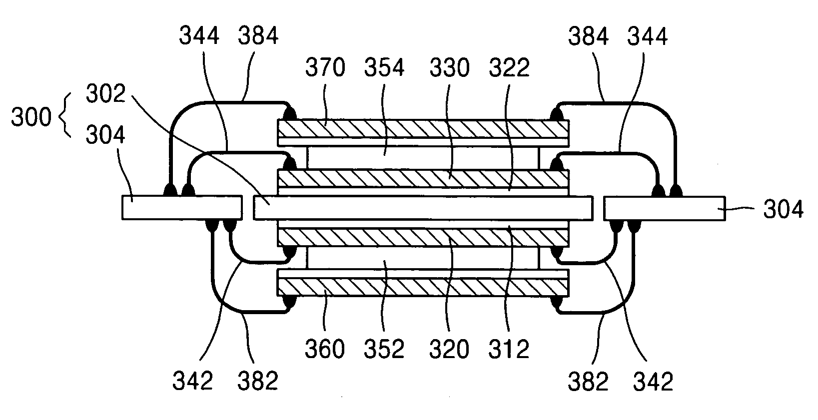
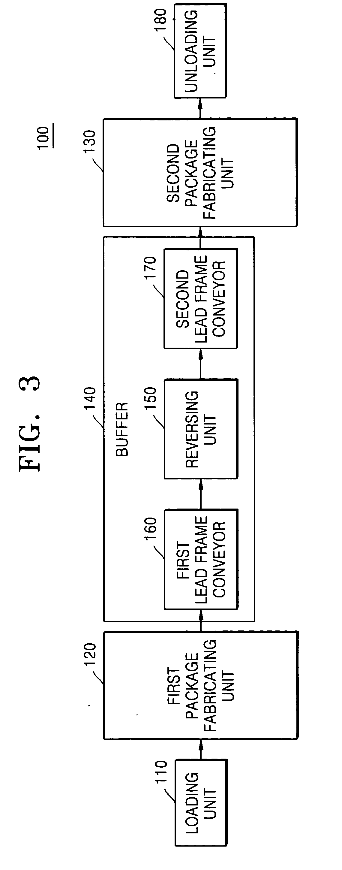
[0044]FIG. 3 is a block diagram illustrating an in-line integrated circuit chip packaging apparatus according to a first exemplary embodiment of the present invention. Referring to FIG. 3, an exemplary in-line integrated circuit chip packaging apparatus 100 includes a loading unit 110 to which a lead frame is supplied in a supply magazine, and first and second package fabricating units 120 and 130 that perform predet...


PUM


Abstract

Provided are in-line semiconductor chip packaging apparatuses that include a buffer assembly in which a reversing unit rotates a lead frame 180° between die attaching and / or wire bonding operations and methods of manufacturing an integrated circuit chip package using such an in-line integrated circuit chip packaging apparatus. Between packaging process operations, the lead frame, which includes first and second surfaces may be rotated, thereby reversing the orientation of the first and second surfaces. The apparatuses will include one or more processing units for attaching semiconductor chips to the leadframe, or a previously mounted semiconductor chip, or for forming wire bonds between the attached semiconductor chip(s) and the corresponding lead fingers of the lead frame, attached to and / or separated by an in-line buffer assembly that includes a reversing unit.

Description

BACKGROUND OF THE INVENTION [0001] This application claims priority from Korean Patent Application No. 2003-44252, which was filed on Jul. 1, 2003, in the Korean Intellectual Property Office, the disclosure of which is incorporated herein in its entirety by reference. [0002] 1. Field of the Invention [0003] The present invention relates to an in-line integrated circuit chip packaging apparatus and a method for manufacturing in-line integrated circuit chip packages and, more particularly, to an in-line integrated circuit chip packaging apparatus for manufacturing a double-sided stacked multi-chip packages using wire bonding techniques and a method of manufacturing integrated circuit chip packages using the same. [0004] 2. Description of the Related Art [0005] The continuing demand for improvements in mobile phones and other personal electronics such as PDAs, MP3 players, digital cameras and notebook computers, has resulting in a corresponding demand for electronic devices that are sm...

Claims


Application Information

Patent Timeline
Patent Type & Authority Applications(United States)
IPC IPC(8): H01L25/18H01L21/50H01L21/677H01L23/495H01L25/065H01L25/07
CPCH01L21/677H01L2224/49113H01L24/49H01L24/85H01L24/92H01L2224/32145H01L2224/32245H01L2224/48091H01L2224/48095H01L2224/48247H01L2224/48463H01L2224/49H01L2224/73265H01L2224/85H01L2224/92H01L2224/92247H01L2924/01004H01L2924/01006H01L2924/01082H01L2924/14H01L24/48H01L2924/00014H01L2924/01033H01L23/49575H01L2224/78H01L2924/00H01L24/45H01L2224/451H01L2924/181H01L2924/00015H01L2224/45099H01L2924/00012H01L2224/05599H01L21/50
Inventor KIM, TAE-HYUNSUN, YOUNG-KYUNKIM, HYUN-HOWOO, JUNG-HWAN
Owner SAMSUNG ELECTRONICS CO LTD
Why Eureka
Try Eureka