Integrated multiplexer/de-multiplexer for active-matrix display/imaging arrays

a technology of active matrix and imaging array, which is applied in the direction of cathode-ray tube indicators, instruments, electric digital data processing, etc., can solve the problems of electrical stress induced meta-stability of tfts, which are not usually used in driving circuit implementation, and achieve the effect of ensuring the stability of transistors

Active Publication Date: 2005-01-13
IGNIS INNOVATION
View PDF25 Cites 19 Cited by
  • Summary
  • Abstract
  • Description
  • Claims
  • Application Information

AI Technical Summary

Benefits of technology

[0014] According to the invention, gate de-multiplexers and read-out multiplexers can be integrated into arrays, such as active-matrix display / imaging arrays, and the integrated gate de-multiplexers and read-out multiplexers can ensure stability of the transistor.

Problems solved by technology

In a-Si:H and polycrystalline silicon, the TFTs suffer from electrical-stress induced meta-stability problems.
Therefore, they are not usually used in the implementation of the driving circuitry.

Method used


Image

  • Integrated multiplexer/de-multiplexer for active-matrix display/imaging arrays
  • Integrated multiplexer/de-multiplexer for active-matrix display/imaging arrays
  • Integrated multiplexer/de-multiplexer for active-matrix display/imaging arrays

Examples


Embodiment Construction

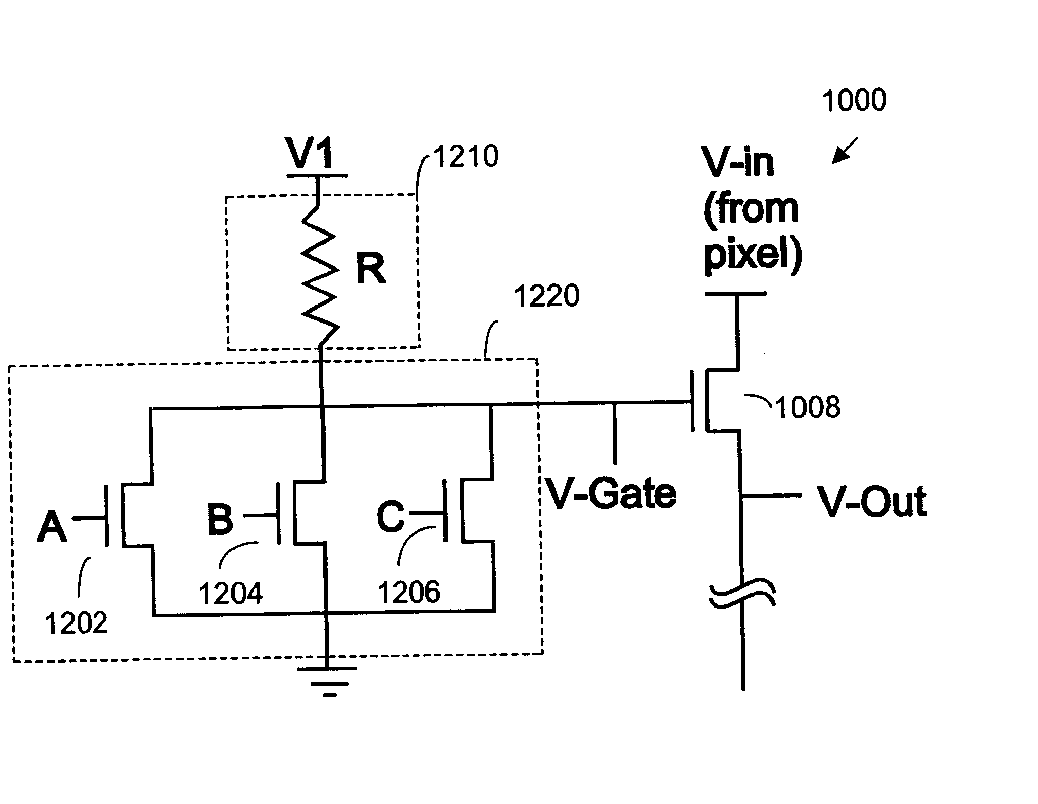
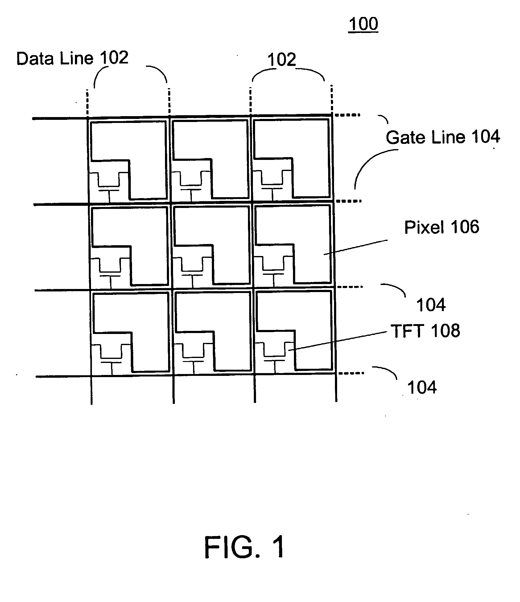
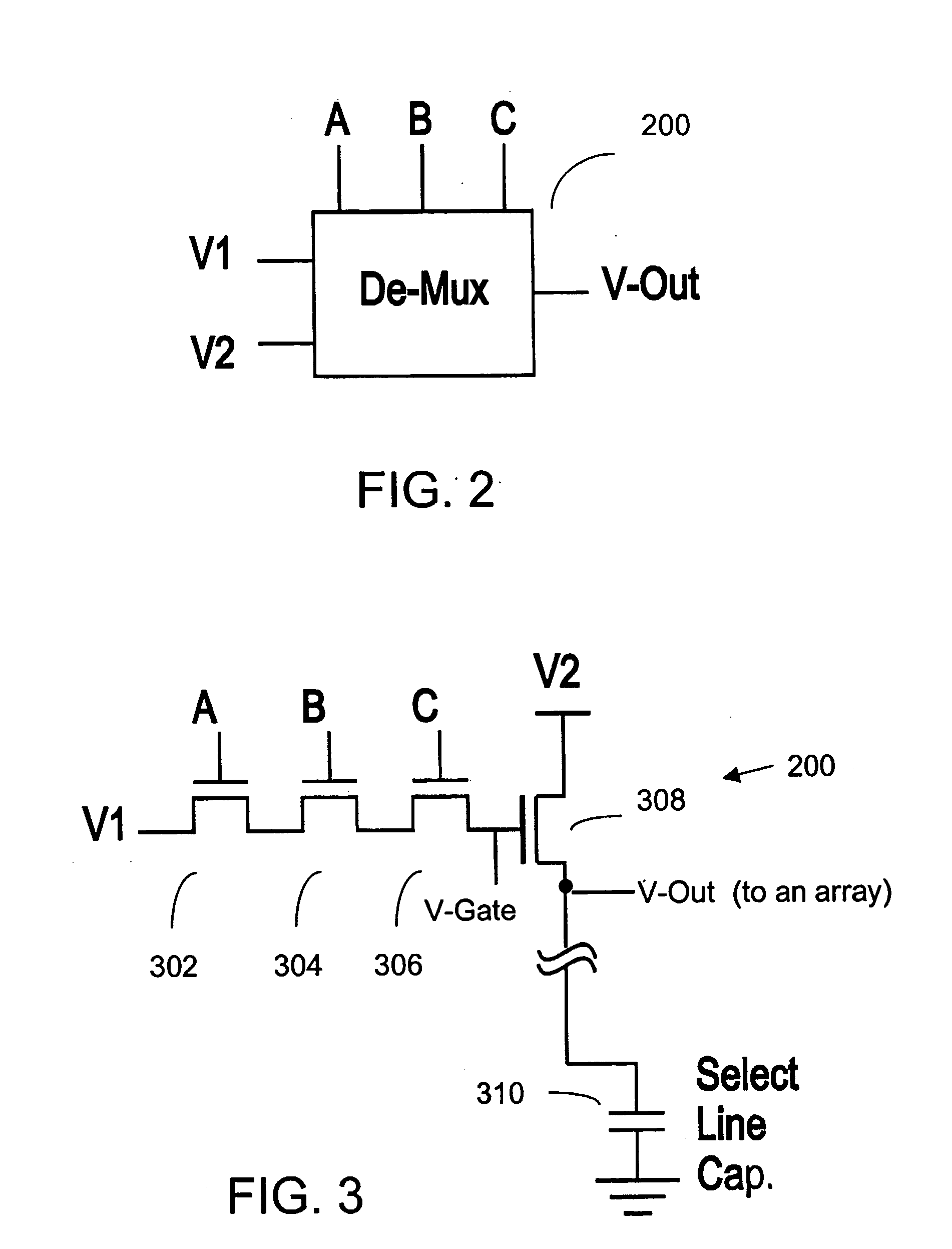
[0034] A gate de-multiplexer circuit block 200 in accordance with one embodiment of the present invention is presented in FIG. 2. The gate de-multiplexer circuit block 200 has terminals V1 and V2, control terminals A, B and C and an output terminal V-Out. As described below, the output terminal V-Out may be connected to a gate line that activates a switching transistor of a pixel. The gate de-multiplexer circuit block 200 includes a plurality of TFTs, which may be a-Si:H, poly-crystalline silicon, or organic / polymer TFTs. The TFTs are connected in series, and whose gate terminals are controlled by external control signals A, B, and C. The gate de-multiplexer 200 can be fabricated on the pixel arrays.

[0035]FIG. 3 shows one example of the gate de-multiplexer circuit block 200 of FIG. 2. In FIG. 3, the gate de-multiplexer includes TFTs 302, 304 and 306 that are connected in series.

[0036] The gates of the TFTs 302, 304 and 306 are connected to the control lines A, B, C, respectively. ...


PUM


Abstract

This invention presents Vt-shift invariant integrated multiplexer and de-multiplexer circuits that can be fabricated with a-Si:H, poly-crystalline silicon, or organic / polymer TFTs. The de-multiplexer and multiplexer includes a plurality of TFTs which are connected in series, and a drive TFT. These circuits are used with active matrix displays to control the gate addressing, and with imaging arrays to multiplex the read-out data.

Description

FIELD OF THE INVENTION [0001] This invention relates in general to an apparatus for reading and / or writing data in active matrix display and imaging arrays. The active matrix can be derived from both inorganic and organic materials that are amorphous or polycrystalline. BACKGROUND OF THE INVENTION [0002] The most popular addressing method in large area displays is active matrix addressing where the gate and data lines form the rows and columns of the grid-like structure. [0003]FIG. 1 is a diagram showing an active matrix array 100 of an active matrix display. The active matrix array 100 has a plurality of pixels 106. The pixels are controlled by transistors in the electronic backplane. The active matrix array has at least one transistor per pixel that acts as an analog switch. The switching transistor either enables or disables writing of data to that pixel. In FIG. 1, Thin Film Transistor (TFT) 108 is shown as the switching transistor, which is connected to a data line 102 and a ga...

Claims


Application Information

Patent Timeline
Patent Type & Authority Applications(United States)
IPC IPC(8): G09G3/36
CPCG09G3/3677
Inventor NATHAN, AROKIAKARIM, KARIM S.MOHAN, NITINKUMAR, ANILSAKARIVA, KAPIL
Owner IGNIS INNOVATION
Why Eureka
Try Eureka