Method for fabricating thin film pattern, method for fabricating device, electro-optical apparatus, and electronic apparatus

a thin film pattern and manufacturing method technology, applied in the direction of conductive pattern formation, identification means, instruments, etc., can solve the problems of generating puddles (bulges) of liquid, high production costs, and most materials, and achieve the effect of reducing the liquid-repellency of the surface at this part and being easy to adjus

Inactive Publication Date: 2005-01-13
SEIKO EPSON CORP
View PDF20 Cites 37 Cited by
  • Summary
  • Abstract
  • Description
  • Claims
  • Application Information

AI Technical Summary

Benefits of technology

[0016] The intermediate drying step can include a heat treatment process or an light irradiation treatment process to dry suitably the function liquids disposed on the substrate. The content of the liquid components left in the function liquids on the substrate can be easily adjusted by conditions for the heat treatment process or an light irradiation treatment process.
[0017] In the method for fabricating a thin film pattern according to the present invention, after the intermediate drying step, a liquid-repelling process, in which the banks are made to be liquid-repellent, can be performed. According to the present invention, on disposing the liquid droplets of the function liquids between the banks, some of the liquid droplets ejected may make contact with, a part of the bank e.g., its upper surface, and therefore, the liquid-repellency of those surfaces at this part may become lowered. In this case, when next ejected liquid droplets of the function liquids put on the part, the liquid droplets cannot flow down smoothly and may damage the film pattern. However, since the banks have liquid repellency by performing the liquid-repelling step before the next material disposing step to apply the liquid-repellency to the banks, even though a part of the liquid droplet ejected is placed on the banks, it is repelled from the banks because of the liquid re

Problems solved by technology

In this photolithography process, large facilities such as vacuum equipment and complicated processes are necessary, efficiencies in the use of materials are around a few percent, that is, most of the materials is discarded, and production costs

Method used


Image

  • Method for fabricating thin film pattern, method for fabricating device, electro-optical apparatus, and electronic apparatus
  • Method for fabricating thin film pattern, method for fabricating device, electro-optical apparatus, and electronic apparatus
  • Method for fabricating thin film pattern, method for fabricating device, electro-optical apparatus, and electronic apparatus

Examples


Embodiment Construction

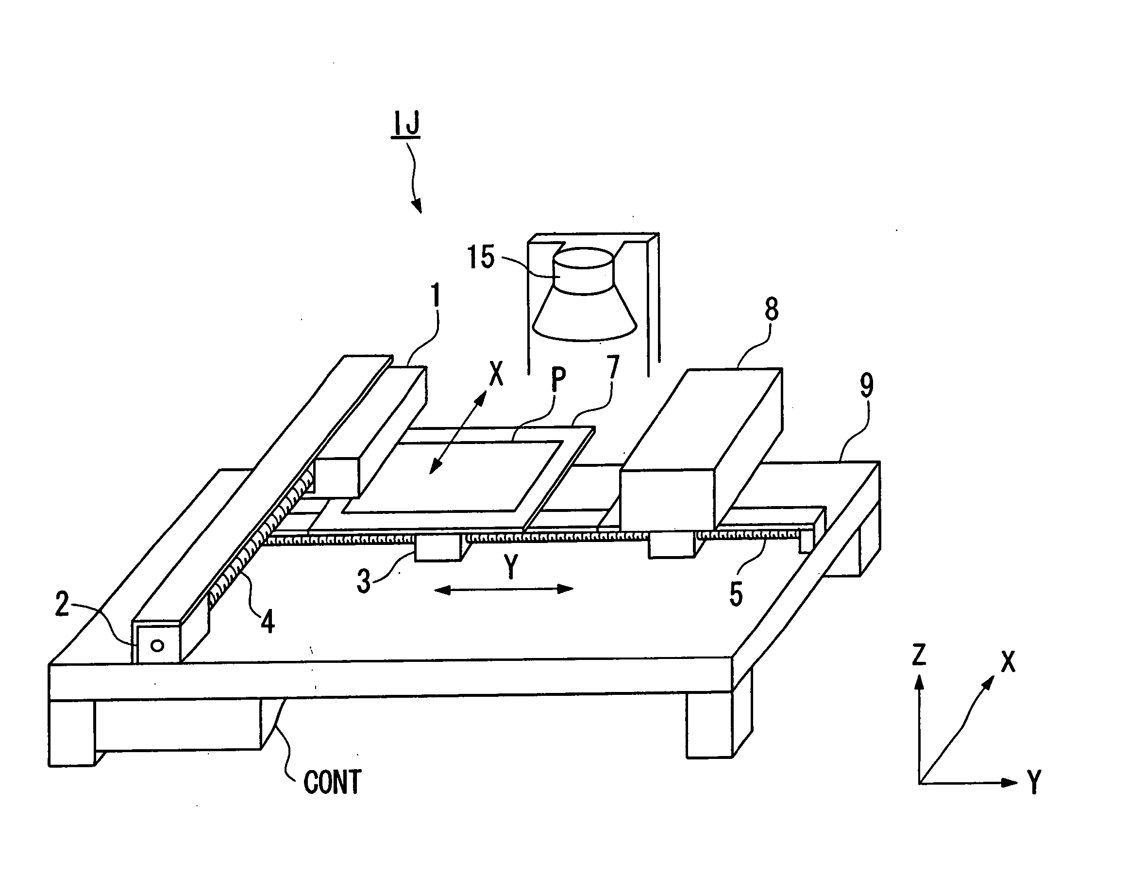
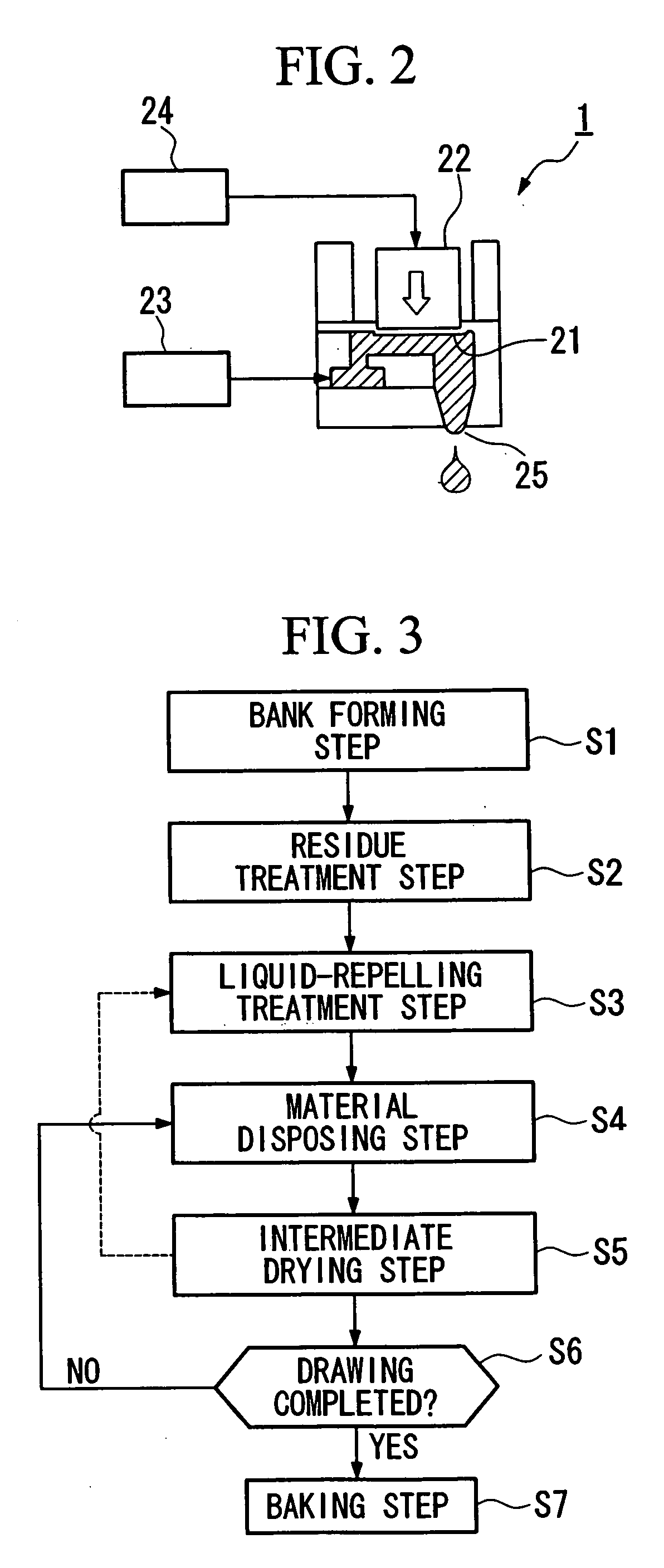
[0047] An embodiment of a method for fabricating a thin film pattern on a substrate and a method for manufacturing a device, according to the present invention, will be explained with reference to the figures. As an example of this embodiment, a case in which an ink (function liquid) for forming patterns of lines (patterns of thin films), in which conductive fine particles are included, is ejected on a substrate in the form of liquid droplets from nozzles of an ejecting head using a liquid droplet ejecting process, and line patterns formed of conductive films on the substrate, will be explained.

[0048] First, an ink (function liquid) which is used is explained. The ink for line patterns of a liquid material, is made of a dispersion liquid, which includes a dispersion medium and conductive fine particles that are dispersed in the dispersion medium, or a solution in which organosilver compound or silver oxide nanometer particles are dispersed (or dissolved) in a solvent (dispersion me...


PUM


Abstract

A method for fabricating a thin film pattern on a substrate includes a bank forming step of forming banks in a predetermined pattern on said substrate, a first material disposing step of disposing first liquid droplets made of a function liquid between said banks to form a first pattern, a second material disposing step of disposing second liquid droplets made of a function liquid on said first pattern, and an intermediate drying step of removing at least a part of a solvent contained in said first liquid droplets between said first material disposing step and said second material disposing step.

Description

BACKGROUND OF THE INVENTION [0001] 1. Field of the Invention [0002] The present invention relates to a method for fabricating a thin film pattern, a method for manufacturing a device, an electro-optical apparatus, and an electronic apparatus. [0003] Priority is claimed on Japanese Patent Application No. 2003-155861, filed May 30, 2003, and Japanese Patent Application No. 2004-94527, filed Mar. 29, 2004, the contents of which are incorporated herein by reference. [0004] 2. Description of Related Art [0005] A photolithography process is used in manufacturing a device with lines (wiring) such as electronic circuits and integrated circuits. In this photolithography process, line patterns of thin films are formed by applying a photosensitive material, a so-called resist, on a conductive film preliminarily applied on a substrate, irradiating the resist in a circuit pattern and developing, and etching the conductive film in the resist pattern. In this photolithography process, large facili...

Claims


Application Information

Patent Timeline
IPC IPC(8): G02F1/1343G02F1/1345G02F1/1362G02F1/1368G09F9/00G09F9/30H01L21/208H01L21/28H01L21/288H01L21/3205H01L21/336H01L21/77H01L21/84H01L27/12H01L27/32H01L29/786H01L51/00H01L51/40H01L51/50H01L51/56H05B33/10H05B33/12H05K3/12
CPCG02F2001/136295H01L21/288H01L27/12H01L27/14687H01L27/1292H01L27/3295H01L51/0005H01L51/0021H05K3/1241H01L27/3244G02F1/136295H10K71/135H10K59/122H10K71/60H10K59/12H01L27/1214
Inventor HIRAI, TOSHIMITSU
Owner SEIKO EPSON CORP
Why Eureka
Try Eureka