

Method of manufacturing a semiconductor device
a manufacturing method and semiconductor technology, applied in the direction of semiconductor devices, basic electric elements, electrical appliances, etc., can solve the problems of easy cracking and difficult to weaken and achieve the effect of easy cracking and weakening the adhesive strength in a short period of tim
- Summary
- Abstract
- Description
- Claims
- Application Information
AI Technical Summary
Benefits of technology
Problems solved by technology
Method used
Image

Examples
embodiment 1
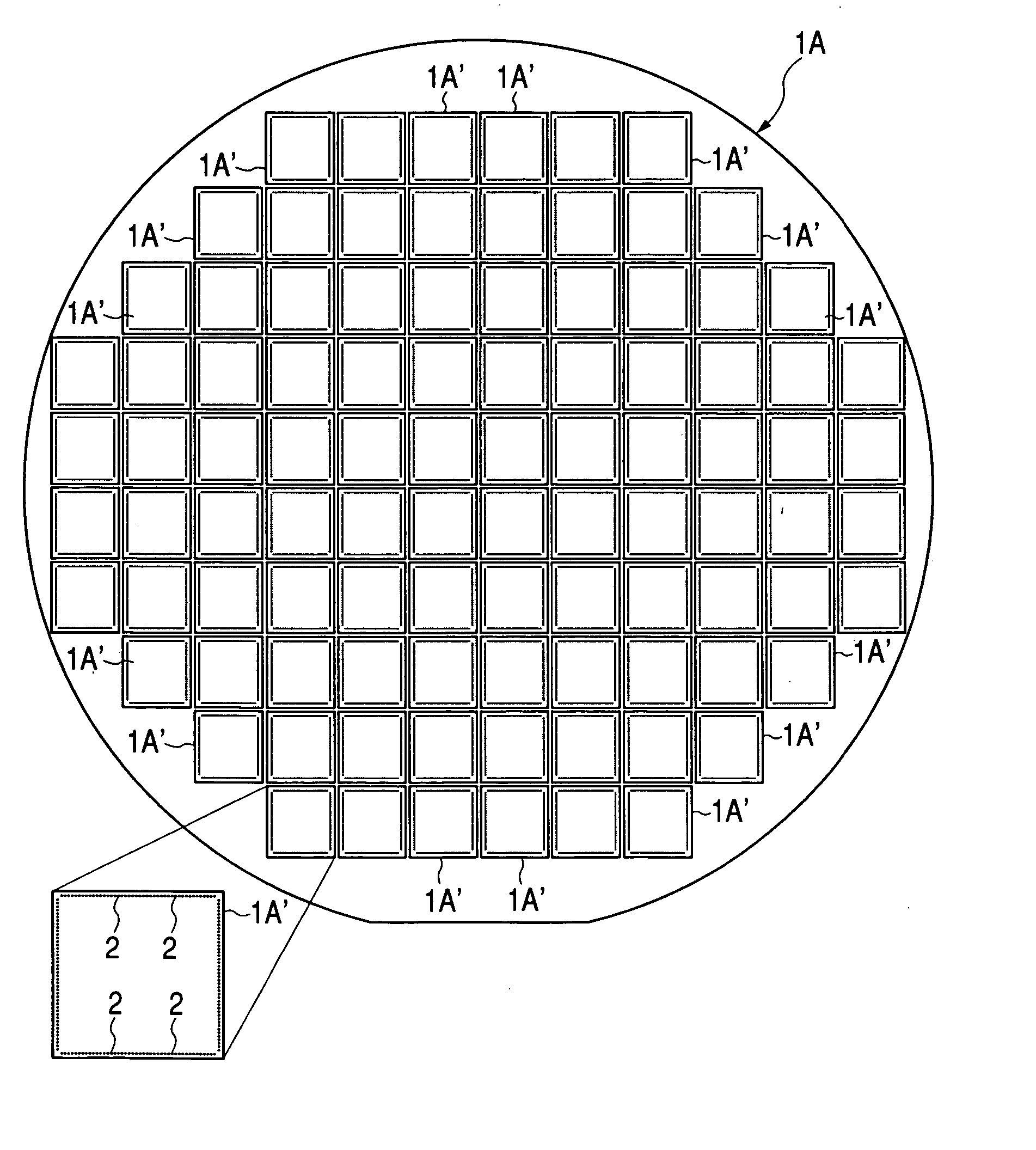
[0047] This embodiment is to be applied to the manufacture of a stacked package in which a plurality of chips are three-dimensionally mounted on a printed wiring board. A method of manufacture of the stacked package will be explained in the order of the steps thereof in conjunction with FIG. 1 to FIG. 23.
[0048] First of all, an integrated circuit is formed over a main surface of a wafer 1A that is made of single crystal silicon, as shown in FIG. 1, in accordance with a well-known manufacturing process; and, thereafter, an electric test is performed by bringing probes into contact with bonding pads 2 on a plurality of chip forming regions 1A′, which are defined by grid-like scribe lines, so as to judge whether respective chip forming regions 1A′ are defective or non-defective.
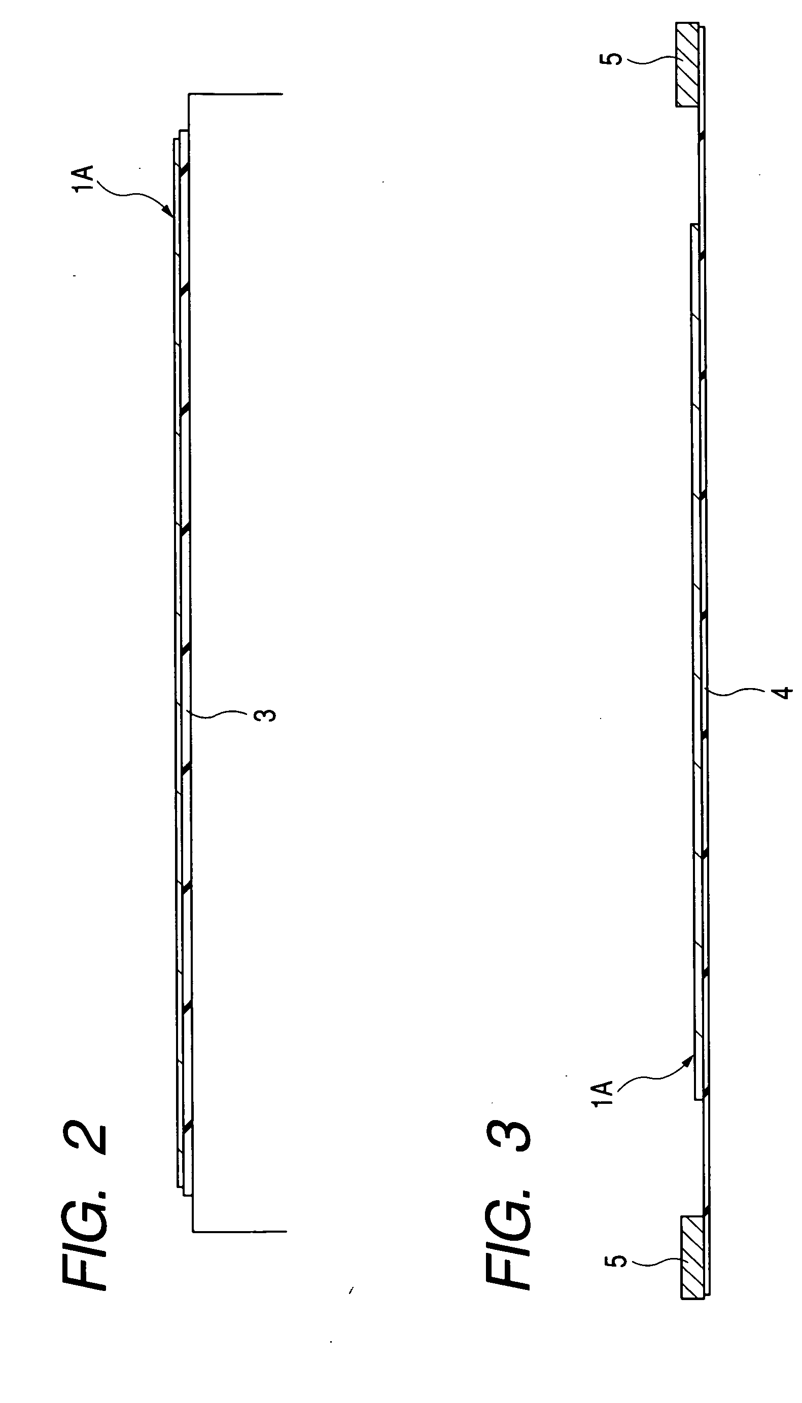
[0049] Next, as shown in FIG. 2, a back grind tape 3, for protecting the integrated circuit, is laminated to the main surface side of the wafer 1A. A back surface of the wafer 1A is ground using a grinder with...
embodiment 2
[0088] The peeling of the chip 1 may be performed in accordance with the timing shown in FIG. 24. To peel the chip 1 in accordance with the timing shown FIG. 24, first of all, as shown in FIG. 25, the suction block 102 is elevated so as to bring an upper surface of the suction block 102 into contact with the back surface of the dicing tape 4, which is positioned below the chip 1 to be peeled, and to suck the dicing tape 4. Here, in the abovementioned embodiment 1, the suction collet 105 is lowered to bring the bottom surface thereof into contact with the upper surface of the chip 1 to be peeled. In this embodiment, however, the suction collet 105 is lowered to the vicinity of the upper surface of the chip 1 and is stopped without bringing the bottom surface of the suction collet 105 into contact with the chip 1 (timing a in FIG. 25).
[0089] Next, as shown in FIG. 26, the vibrator 110 is elevated to bring the head 111a into contact with the back surface of the dicing tape 4; and, at ...
PUM
 Abstract
Description
Claims
Application Information