

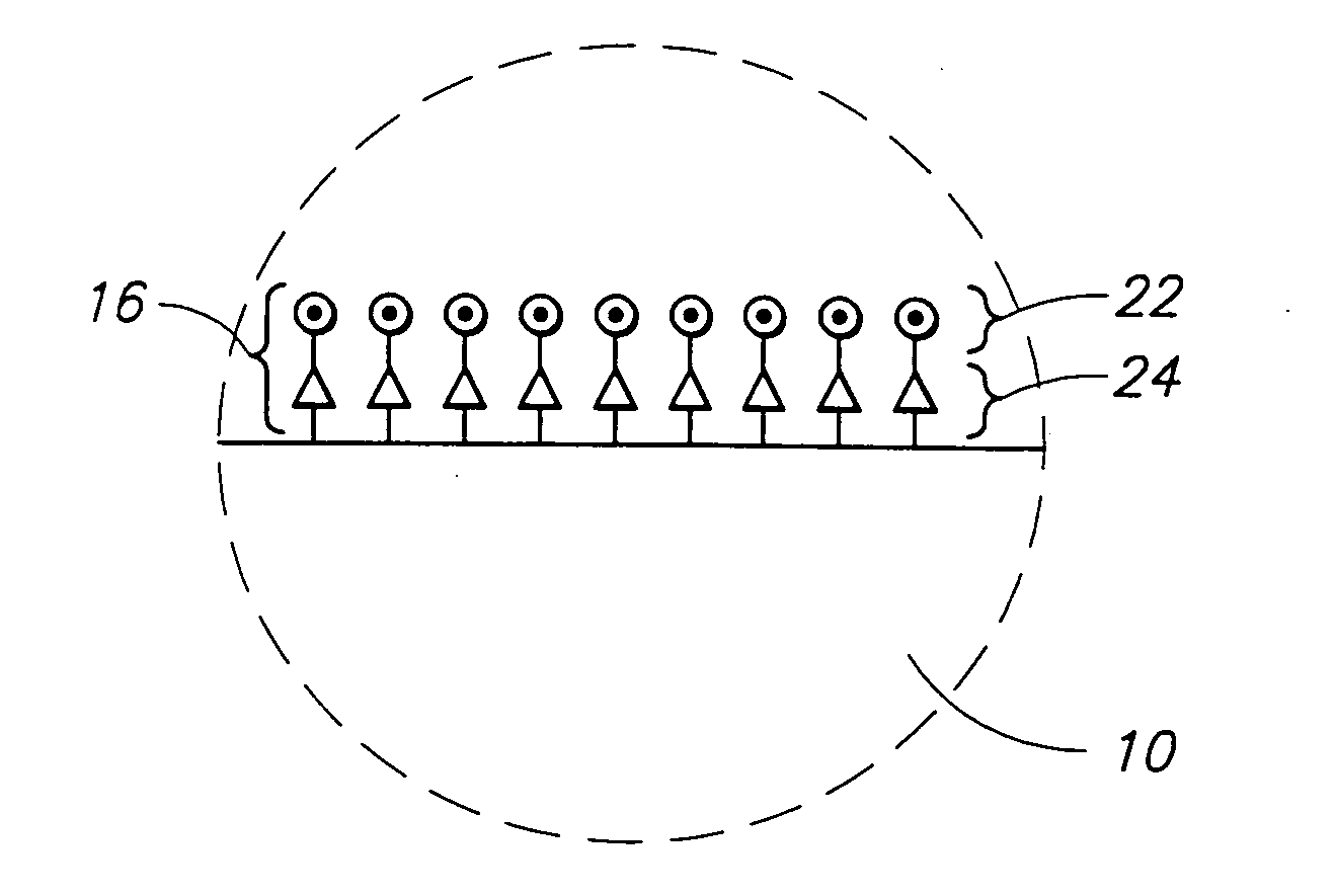
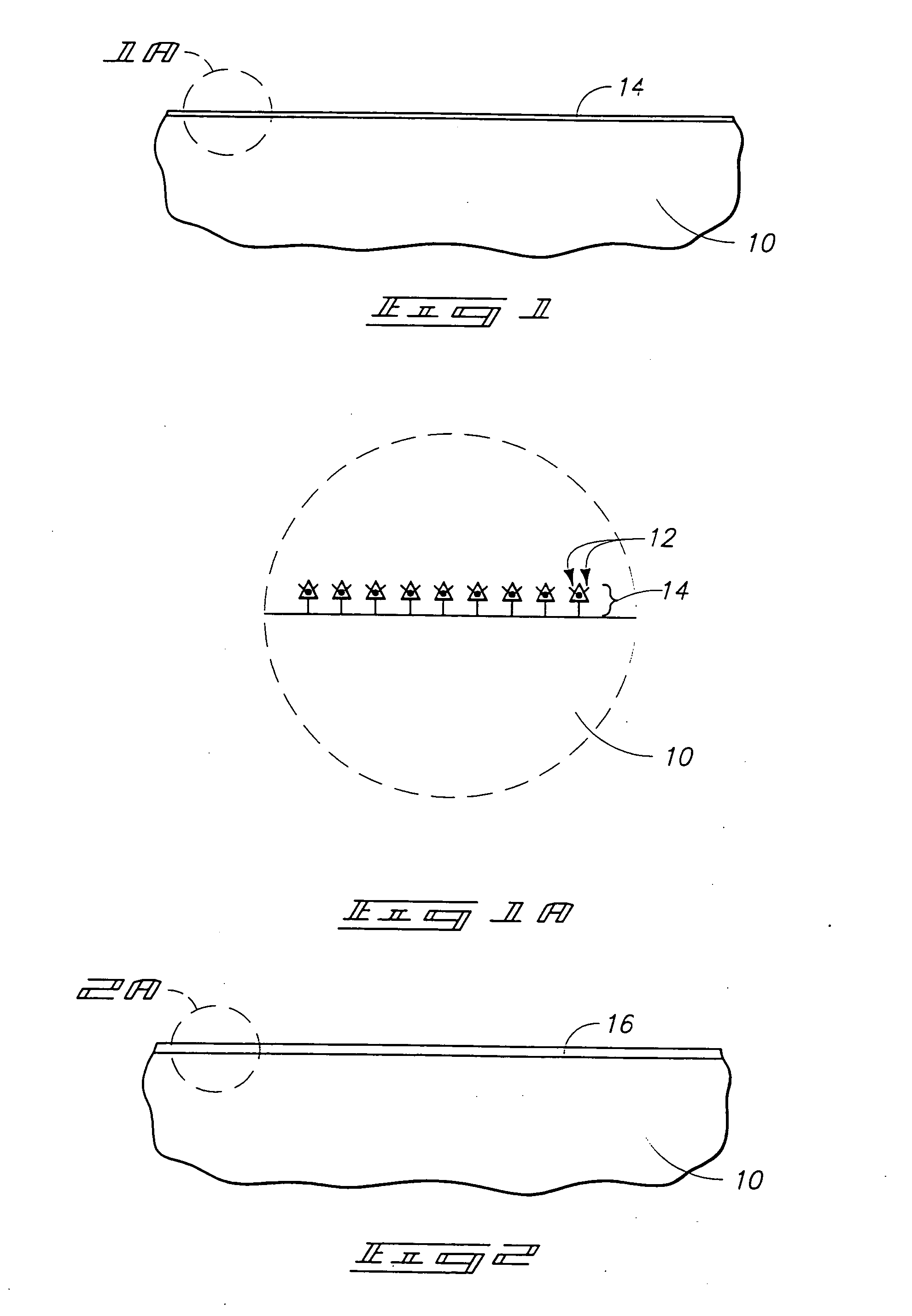
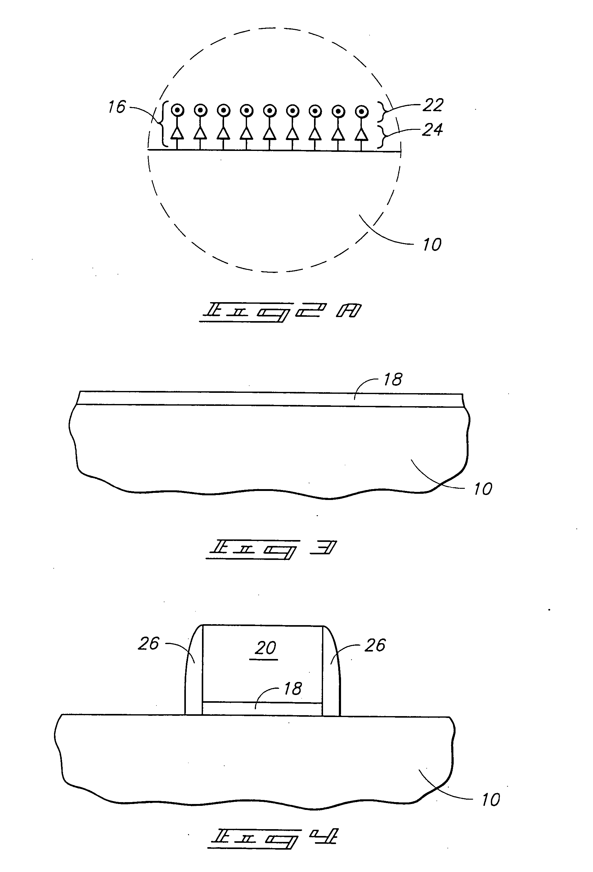
Composite dielectric forming methods and composite dielectrics
a technology of composite dielectrics and dielectric forming methods, which is applied in the direction of coatings, semiconductor devices, chemical vapor deposition coatings, etc., can solve the problems of reducing the output of transistors, forming and using ultra-thin siosub>2/sub>layers, and reducing the capacitance or amount of charge such a capacitor can stor
- Summary
- Abstract
- Description
- Claims
- Application Information
AI Technical Summary
Problems solved by technology
Method used
Image

Examples
Embodiment Construction
[0018] Material properties of various high-K dielectric materials for gate dielectrics are discussed in a recent article by G. D. Wilk, et al., High-K Gate Dielectric: Current Status and Materials Properties Considerations, Journal of Applied Physics, vol. 89, no. 10, pp. 5243-5275 (May, 2001). Table 1 summarizes information from Wilk et al.
TABLE 1DielectricBand gapΔ EC (eV)CrystalMaterialConstant (K)EG (eV)to SiStructure(s)SiO23.98.93.2AmorphousSi3N475.12AmorphousAl2O398.72.8AmorphousY2O3155.62.3CubicLa2O3304.32.3Hexagonal, cubicTa2O5264.51-1.5OrthorhombicTiO2803.51.2Tetragonal(rutile, anataseHfO2255.71.5Monoclinic,tetragonal, cubicZrO2257.81.4Monoclinic,tetragonal, cubic
[0019] The inventors recognized the advantage of a composite dielectric containing hafnium oxide and lanthanum oxide as described in U.S. patent application Ser. No. 09 / 881,408, filed Jun. 13, 2001, entitled A Dielectric Layer Forming Method And Devices Formed Therewith, the subject matter of which is incorporate...
PUM
| Property | Measurement | Unit |
|---|---|---|
| width | aaaaa | aaaaa |
| dielectric constant | aaaaa | aaaaa |
| thickness | aaaaa | aaaaa |
Abstract
Description
Claims
Application Information