Nonvolatile semiconductor memory device

Inactive Publication Date: 2005-01-20
RENESAS TECH CORP
View PDF10 Cites 5 Cited by
  • Summary
  • Abstract
  • Description
  • Claims
  • Application Information

AI Technical Summary

Benefits of technology

[0018] In this case, since a negative side voltage is applied to the drain, the electrons are less easily injected into the drain while they are more easily injected into the floating gate. Accor

Problems solved by technology

However, such a stacked gate structure has a complex configuration and thus requires a complex manufacturing process.
As such, it is difficult to provide a large potential difference between the substrate and the floating gate.
However, a memory transistor disclosed in the above two references is an n-channel metal oxide semiconductor (MOS) transistor where data writing at a low voltage is difficult.
Theref

Method used


Image

  • Nonvolatile semiconductor memory device
  • Nonvolatile semiconductor memory device
  • Nonvolatile semiconductor memory device

Examples


first embodiment

[0045] First Embodiment

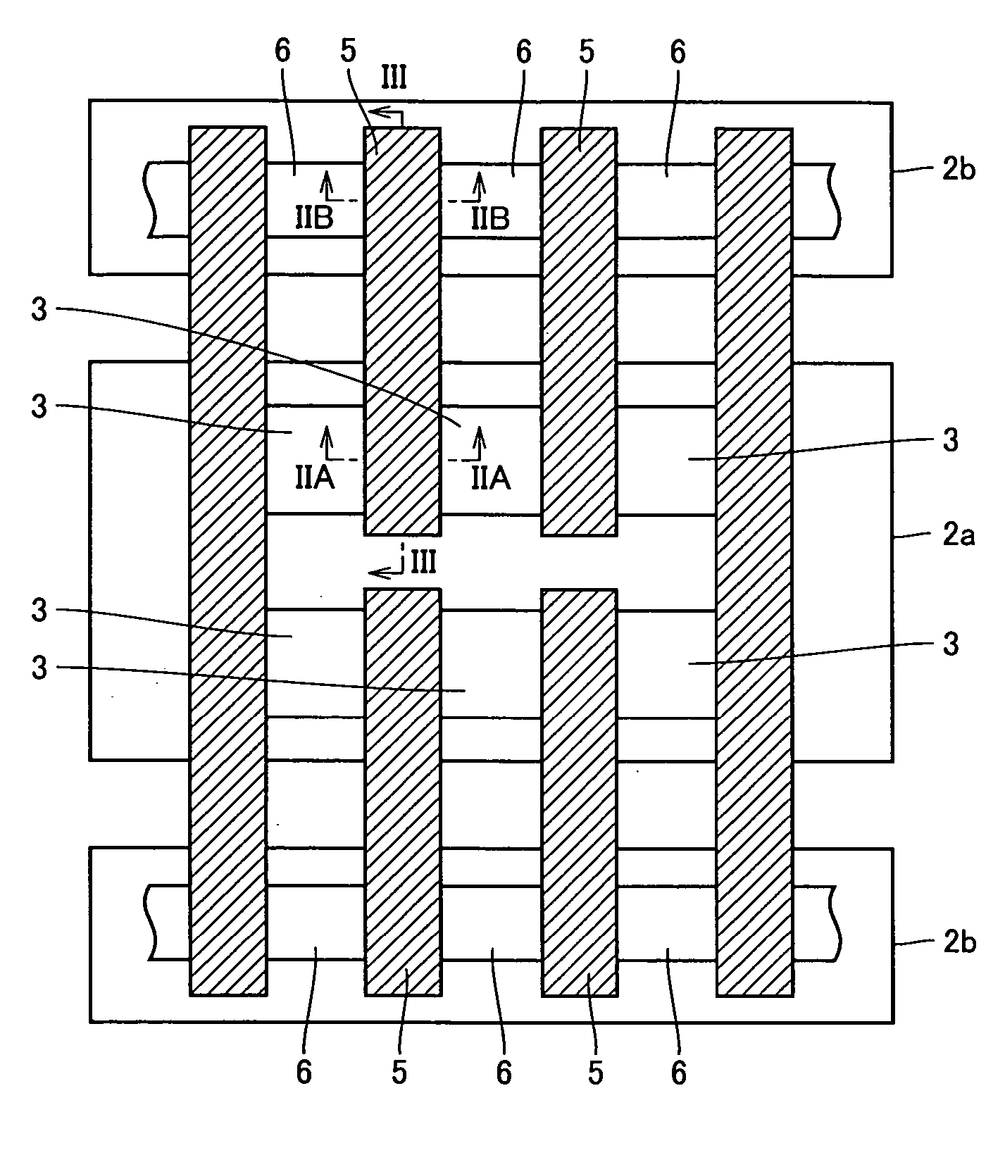
[0046] A selection transistor is not shown except for FIG. 1 and will not be described though it is typically provided for every bit in a memory cell. The reason is that the selection transistor is not related to an operating principle in the embodiment of the present invention. The selection transistor is also treated as such in other embodiments of the present invention.

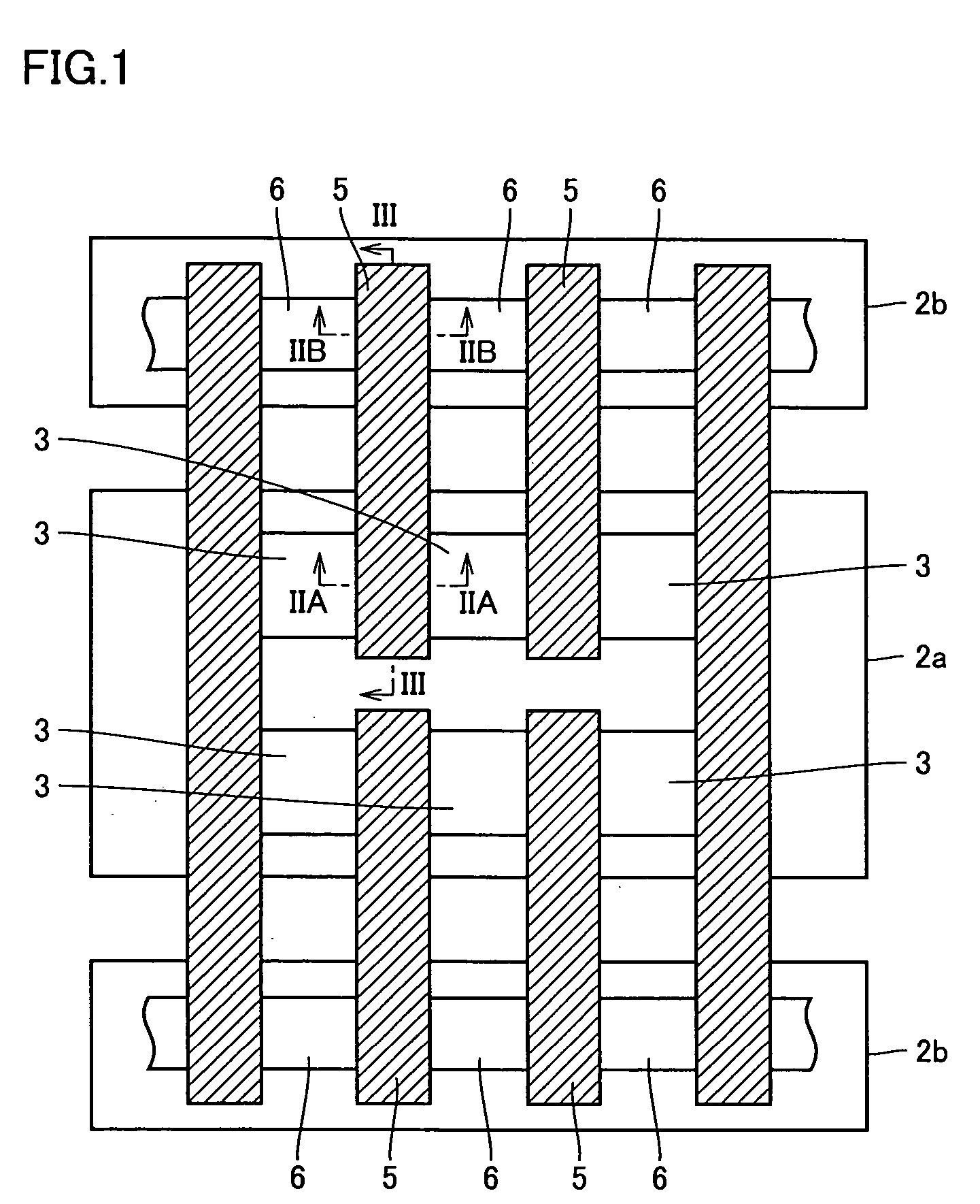
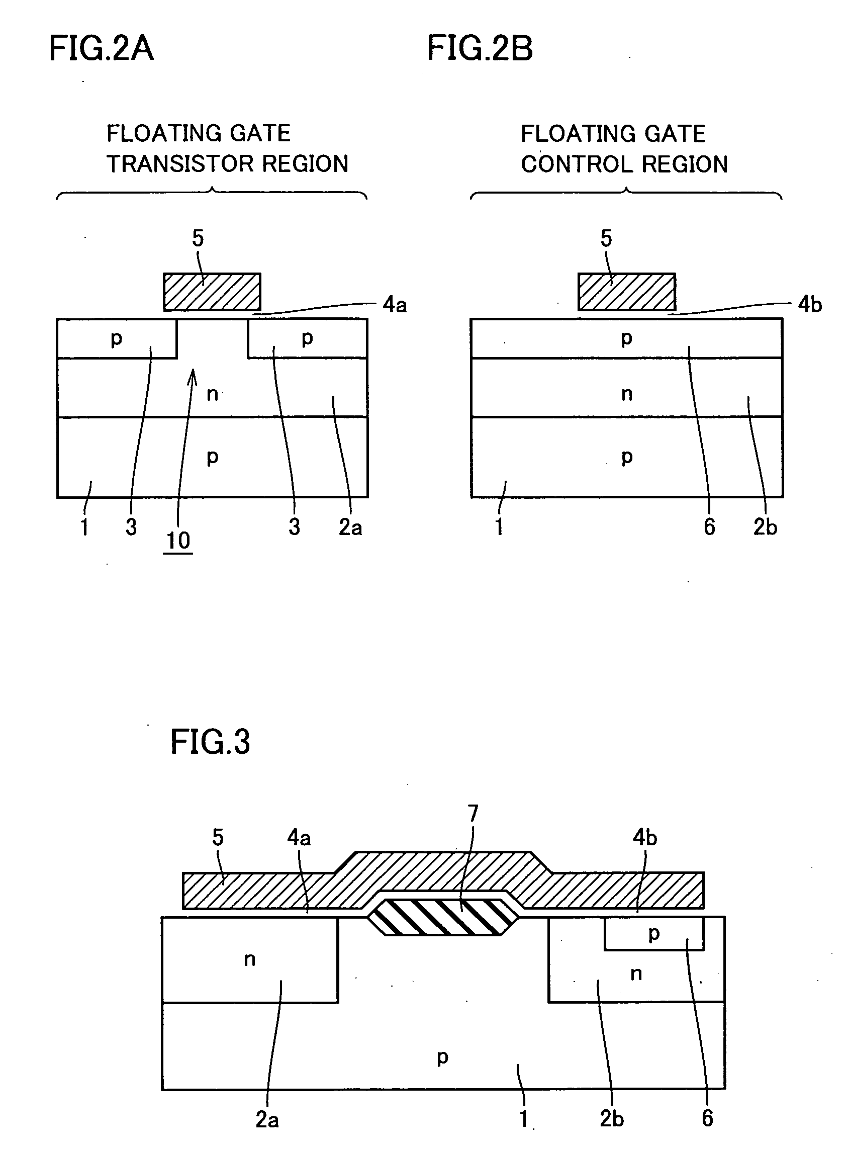
[0047] Referring to FIGS. 1 to 3, a memory cell of the embodiment mainly includes a floating gate transistor 10 and a portion to control a floating gate 5.

[0048] Referring to FIG. 2A, in a region where the floating gate transistor is formed, an n-type well region 2a is formed at a main surface of a p-type semiconductor substrate 1. In n-type well region 2a is formed floating gate transistor 10 which is a p-channel MOS transistor. Floating gate transistor 10 includes a pair of p-type impurity diffused regions 3, 3 which is to serve as the source / drain, a tunnel insulating layer 4a, and float...

second embodiment

[0059] Second Embodiment

[0060] Referring to FIGS. 4 and 5, a configuration of a memory cell of the embodiment differs from that of the first embodiment in that it has a p-type impurity diffused region 8 for device isolation.

[0061] P-type impurity diffused region 8 for device isolation is formed at semiconductor substrate 1 just below field insulating layer 7 which is formed at the main surface of semiconductor substrate 1 between the floating gate transistor region and the floating gate control region. P-type impurity diffused region 8 for device isolation has higher carrier concentration than semiconductor substrate 1.

[0062] Since a configuration except for the aforementioned is almost similar to that of the first embodiment, similar reference characters are given to similar components and description thereof will not be repeated.

[0063] According to the embodiment, the following effect can be obtained.

[0064] In write and erase operations, when a voltage as shown in tables 1 and...

third embodiment

[0066] Third Embodiment

[0067] Referring to FIGS. 6 to 8, a configuration of a memory cell of the embodiment differs from that of the first embodiment in its configuration of an impurity diffused control region in the floating gate control region.

[0068] The impurity diffused control region of the embodiment is configured of a pair of n-type source / drain impurity diffused regions 11, 11. The pair of source / drain impurity diffused regions 11, 11 is formed at the main surface of p-type semiconductor substrate 1 such that a region of semiconductor substrate 1 positioned below floating gate 5 is interposed between the paired source / drain regions. The pair of source / drain impurity diffused regions 11, 11, an insulating layer 4b, and floating gate 5 configure a control transistor 20 which is an n-channel MOS transistor.

[0069] Since a configuration except for the aforementioned is almost similar to that of the first embodiment, similar reference characters are given to similar components a...


PUM


Abstract

A nonvolatile semiconductor memory device includes: a semiconductor substrate having a main surface; a pair of p-type impurity diffused regions, formed at the main surface of the semiconductor substrate to serve as source/drain; a floating gate formed on a region of the semiconductor substrate lying between the paired p-type impurity diffused regions, with a tunnel insulating layer interposed between the floating gate and the region of the semiconductor substrate; and an impurity diffused control region formed at the main surface of the semiconductor substrate to control a potential of the floating gate. Accordingly, a nonvolatile semiconductor device can be obtained in which data can be electrically erased and written at a low voltage.

Description

BACKGROUND OF THE INVENTION [0001] 1. Field of the Invention [0002] This invention relates to a nonvolatile semiconductor memory device. More particularly, this invention relates to a nonvolatile semiconductor memory device having a memory cell of a single layer gate structure. [0003] 2. Description of the Background Art [0004] In a conventional flash memory, a memory cell has a stacked gate structure where a floating gate is formed on a channel region with a tunnel oxide layer interposed therebetween and furthermore a control gate is formed on the floating gate with an insulating film interposed therebetween. However, such a stacked gate structure has a complex configuration and thus requires a complex manufacturing process. [0005] Thus, in order to simplify the configuration and the manufacturing process, a memory cell having a single layer gate structure is proposed where a floating gate is the only gate on a channel region. [0006] In a memory cell having a conventional single la...

Claims


Application Information

Patent Timeline
IPC IPC(8): H01L21/8247H01L27/115H01L29/788H01L29/792
CPCH01L27/115H01L29/7883H01L27/11558H01L27/11521H10B41/60H10B69/00H10B41/30E04G17/14
Inventor ENDO, SEIICHIISHII, MOTOHARU
Owner RENESAS TECH CORP
Why Eureka
Try Eureka