Thin film transistor circuit and semiconductor display device using the same

a thin film transistor and display device technology, applied in static indicating devices, solid-state devices, instruments, etc., can solve the problems of blur in the entire display device, change of threshold value or deterioration, and meaningless buffers, etc., to achieve excellent picture without picture blur, low fluctuation, and high fineness/high resolution

Inactive Publication Date: 2005-01-20
SEMICON ENERGY LAB CO LTD
View PDF12 Cites 13 Cited by
  • Summary
  • Abstract
  • Description
  • Claims
  • Application Information

AI Technical Summary

Benefits of technology

[0029] The present invention has been made to solve the foregoing problems, and an object thereof is to provide a buffer in which even in the case where there is a difference in characteristics of each TFT, these differences of characteristics can be canceled. Another object of the invention is to provide a driver circuit of an active matrix type semiconductor display device, which uses this buffer with little fluctuation. Still another object of the invention is to provide a semiconductor display device using this driver circuit of the invention and capable of obtaining an excellent picture without a picture blur and with high fineness / high resolution.

Problems solved by technology

Such a buffer is meaningless if its current capacity is small, and a buffer having a large current capacity to a certain degree is required.
Further, when the size of a TFT is large, self heat generation of the TFT becomes large, which may cause a change of a threshold value or deterioration to occur.
Thus, as described above, if fluctuation in applied voltage occurs for every source signal line, a display blur in the entire of the display device appears, and excellent display can not be made.
In this case as well, a buffer having a large current capacity is necessary, so that the above described problems come to occur.
Especially, the buffer of the gate signal line must drive all of the connected TFTs for one line in the pixel matrix circuit, so that the fluctuation in the characteristics of the buffer causes a remarkable picture blur.
This is one of the most serious problems when a display device with high fineness / high resolution is desired.

Method used


Image

  • Thin film transistor circuit and semiconductor display device using the same
  • Thin film transistor circuit and semiconductor display device using the same
  • Thin film transistor circuit and semiconductor display device using the same

Examples


embodiment 1

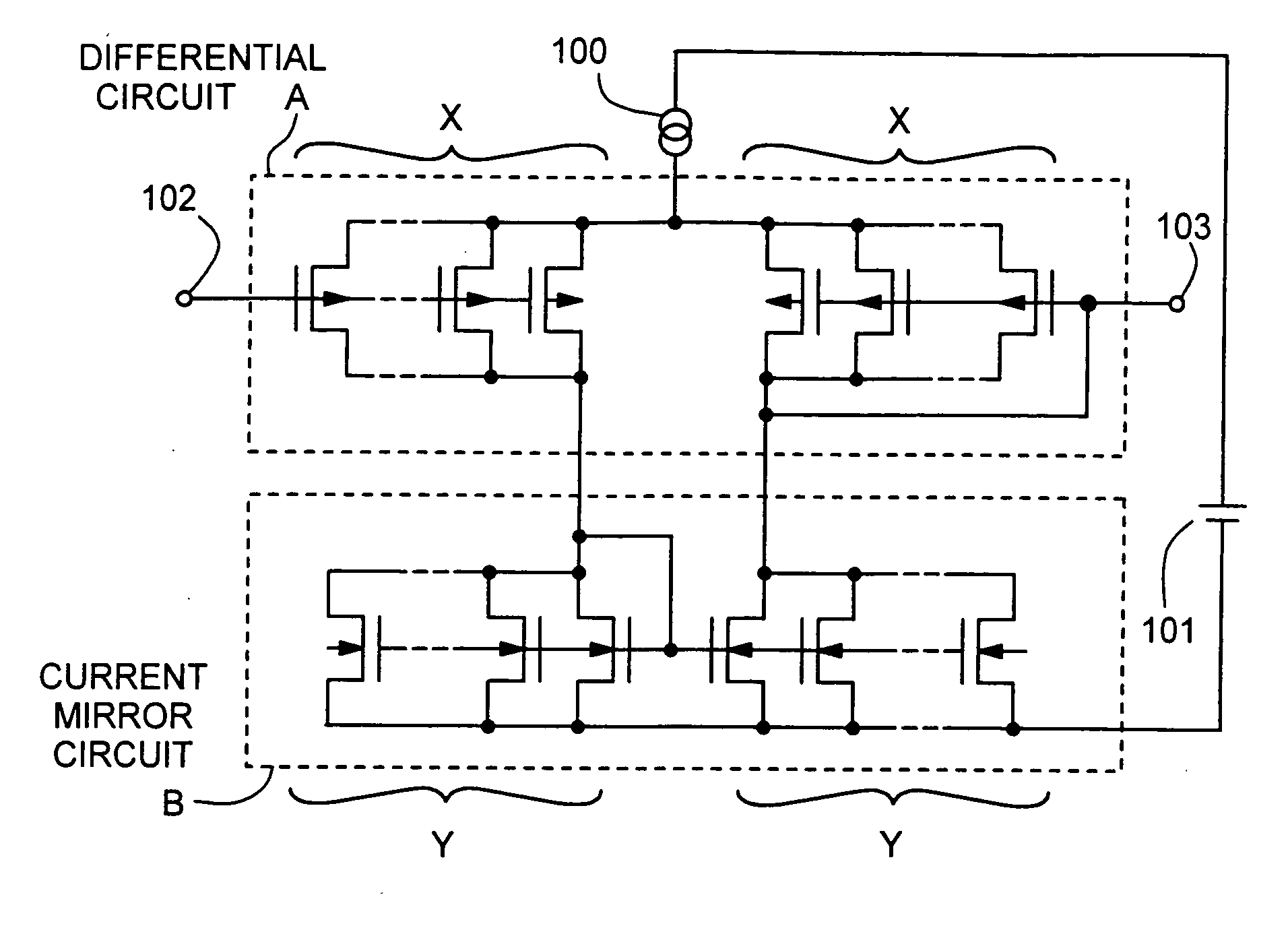
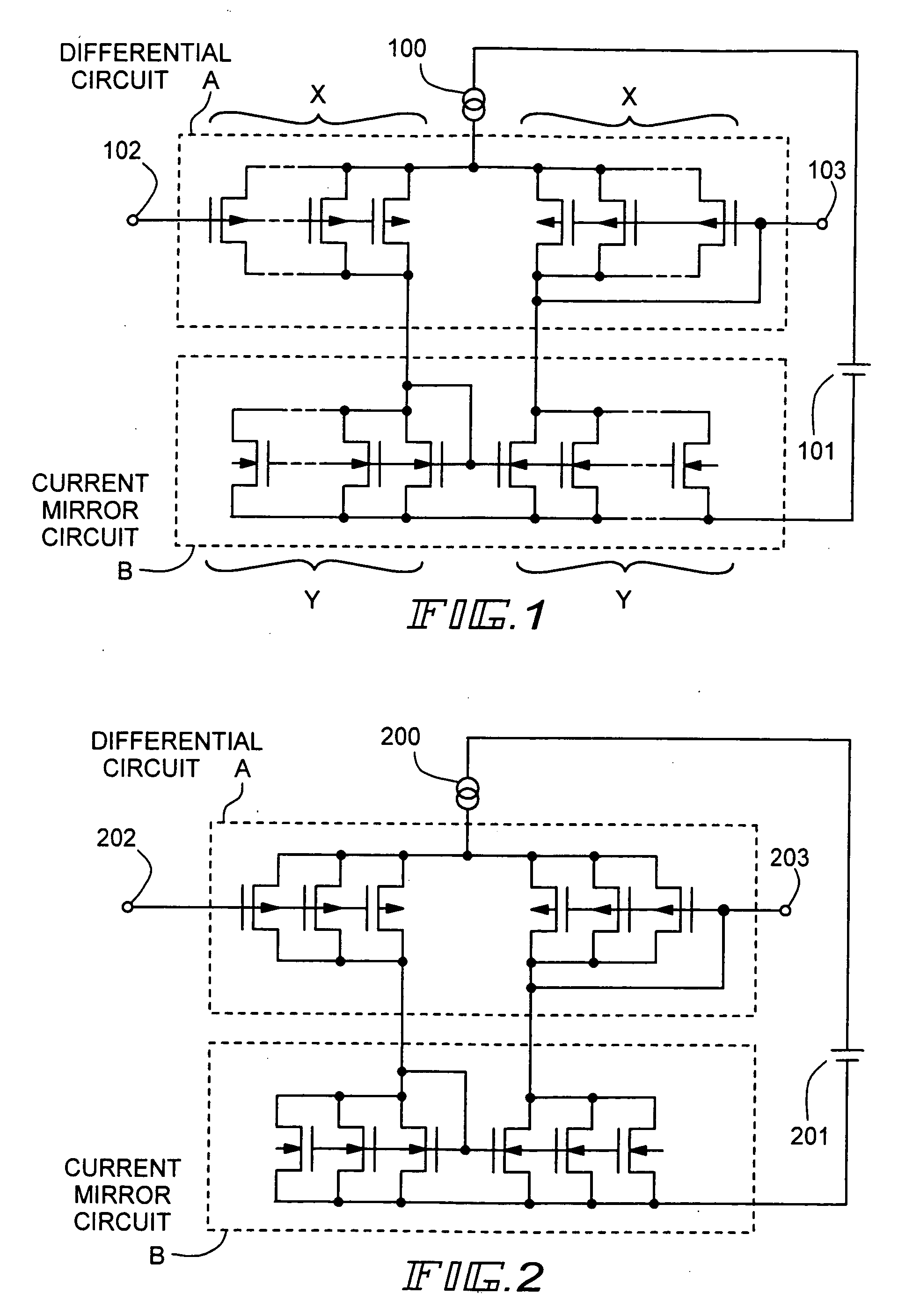
[0051]FIG. 2 shows an embodiment of the present invention. FIG. 2 shows a case where the structure of the present invention is used for an analog buffer of a source signal line side driver circuit of an active matrix type semiconductor display device. In the analog buffer of this embodiment, x=y=3.

[0052] The analog buffer shown in FIG. 2 is constituted of a differential amplifier of a circuit A encircled with a dotted line and a current mirror circuit of a circuit B encircled with a dotted line. The channel width of each of six P-channel TFTs constituting the differential amplifier is 30 μm. The channel width of each of N-channel TFTs constituting the current mirror circuit is 30 μm.

[0053] In this embodiment, although the number of TFTs constituting the differential circuit is equal to the number of TFTs constituting the current mirror circuit, it is not always necessary to make the number equal to each other. Besides, although the channel width of each TFT is 30 μm, it is satisfa...

embodiment 2

[0117]FIG. 8 shows another embodiment of the present invention. FIG. 8 shows a case where the structure of the present invention is used for an analog buffer of a source signal line side driver circuit of an active matrix type semiconductor display device. In this embodiment, the number of output-side thin film transistors of a differential circuit and that of a current mirror circuit are respectively made to be three times as large as that of the foregoing embodiment 1. In other words, the output-side circuits of the differential circuit and the current mirror circuit are respectively multiplied by three. By this, the current capacity of the constructed analog buffer is increased.

[0118] In this embodiment, the channel width of each of 12 P-channel TFTs constituting the differential amplifier is 30 μm. The channel width of each of N-channel TFTs constituting the current mirror circuit is 30 μm. In this embodiment, although the channel width of each TFT is 30 μm, it is appropriate t...

embodiment 3

[0121] The active matrix type liquid crystal display device of the present invention described in the embodiments 1 and 2 can sufficiently be used for an active matrix type liquid crystal display device with high fineness / high resolution, and the number of pixels is so enormous that the device can be applied to a future ATV (Advanced TV). Thus, the present invention can also be used for an active matrix type liquid crystal display device with the resolution of XGA or higher, for example, 1920 horizontal pixels by 1280 vertical pixels.


PUM


Abstract

There is provided a thin film transistor circuit used for a driver circuit for providing a semiconductor display device without a picture blur and with high fineness / high resolution. In the thin film transistor circuit, a TFT having a large size (channel width) is not used, but a plurality of TFTs each having a small size are connected in parallel to each other and are used. By this, while sufficient current capacity of the thin film transistors is secured, fluctuation in the characteristics can be decreased.

Description

BACKGROUND OF THE INVENTION [0001] 1. Field of the Invention [0002] The present invention relates to a driver circuit for a semiconductor display device using thin film transistors. Particularly, the invention relates to a differential amplifying circuit and a buffer using the same, which is used for a driver circuit of an active matrix type semiconductor display device. Moreover, the invention relates to a semiconductor display device using the driver circuit. [0003] 2. Description of the Related Art [0004] In recent years, a technique for manufacturing a thin film transistor (TFT) using a semiconductor thin film formed on an inexpensive glass substrate has been rapidly developed. The reason is that the demand for an active matrix type liquid crystal display device and an electroluminescence (EL) display device has been increased. [0005] In the active matrix type liquid crystal display device, a TFT is disposed for each of several hundred thousands to millions of pixels arranged in...

Claims


Application Information

Patent Timeline
Patent Type & Authority Applications(United States)
IPC IPC(8): G09G3/20G09G3/36H01L21/77H01L21/84H01L27/12H03F3/45
CPCG09G3/2011G09G3/3688G09G2320/02H03F2203/45674H03F3/45183H03F2203/45371H01L27/1214H01L27/124
Inventor YAMAZAKI, SHUNPEIKOYAMA, JUN
Owner SEMICON ENERGY LAB CO LTD
Why Eureka
Try Eureka