Method of fabricating complementary bipolar transistors with SiGe base regions

a bipolar transistor and base layer technology, applied in the direction of basic electric elements, electrical apparatus, semiconductor devices, etc., can solve the problems of limited driver capacity, inability to integrate gallium arsenide transistors, and inability to achieve the bandwidth and available driver capacity, etc., to achieve the effect of simple manner

Active Publication Date: 2005-01-20
TEXAS INSTR INC
View PDF3 Cites 8 Cited by
  • Summary
  • Abstract
  • Description
  • Claims
  • Application Information

AI Technical Summary

Benefits of technology

[0005] The invention is thus based on the objective of providing a method with which the base layers of complementary bipolar transistors can be formed with an optimized germanium profile in a simple manner.

Problems solved by technology

The achievable bandwidth and the available driver capacity is, however, restricted in CMOS processes.
Gallium arsenide transistors do not permit integration, however, in conventional CMOS processes.
Simultaneous epitaxial growth of the base layers of both transistors (NPN and PNP) does not permit optimizing the germanium profile, however.

Method used


Image

  • Method of fabricating complementary bipolar transistors with SiGe base regions
  • Method of fabricating complementary bipolar transistors with SiGe base regions
  • Method of fabricating complementary bipolar transistors with SiGe base regions

Examples


Embodiment Construction

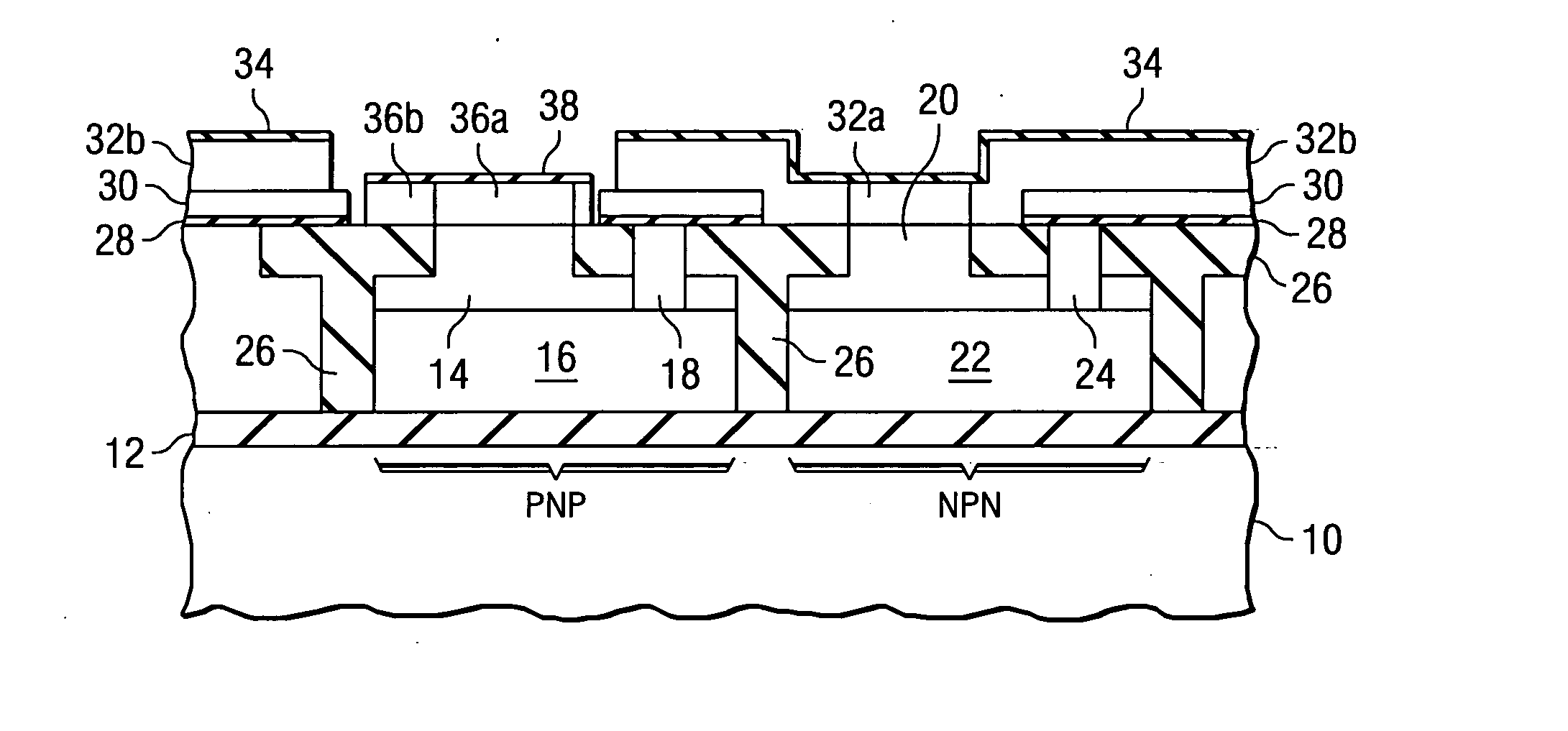
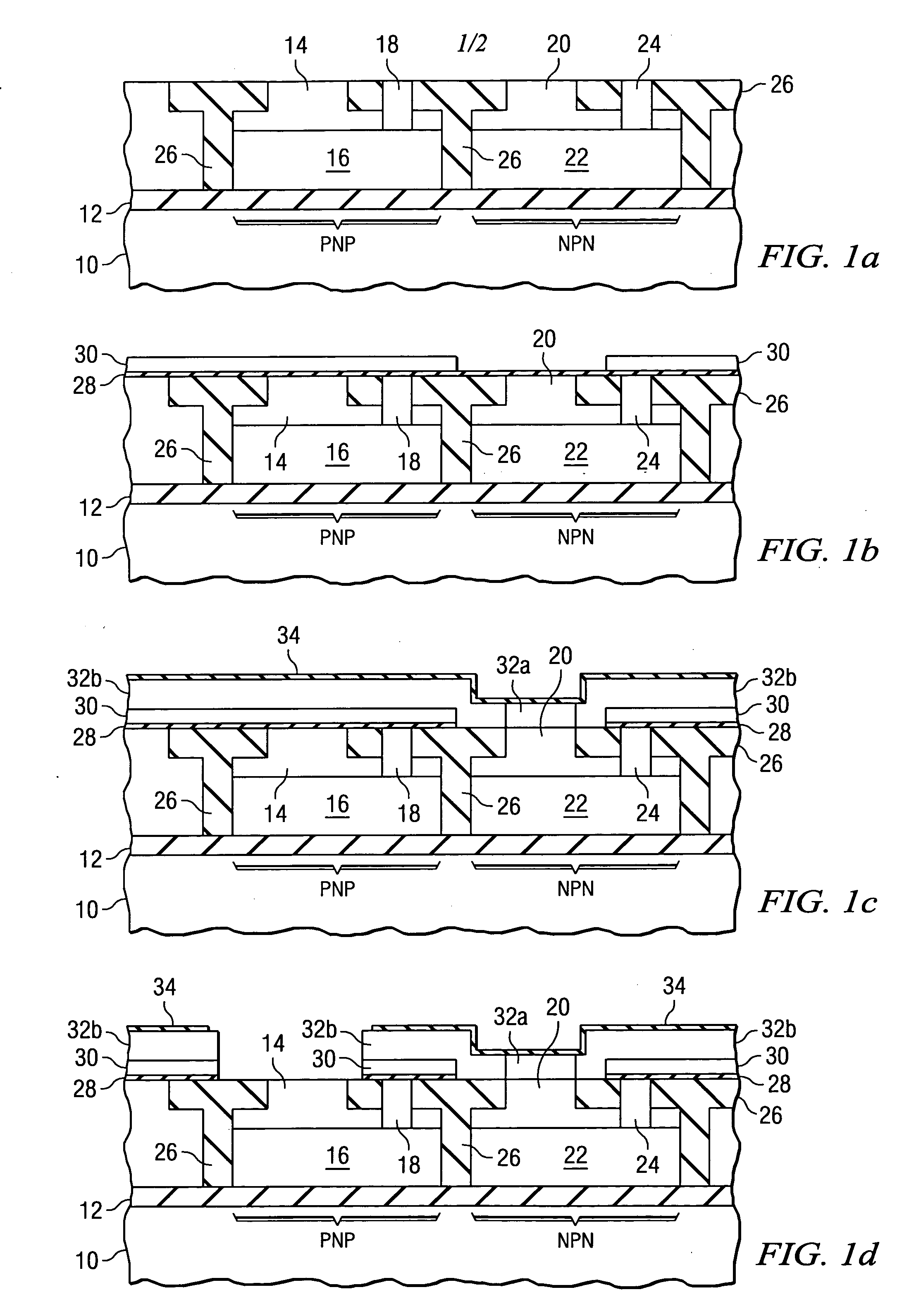
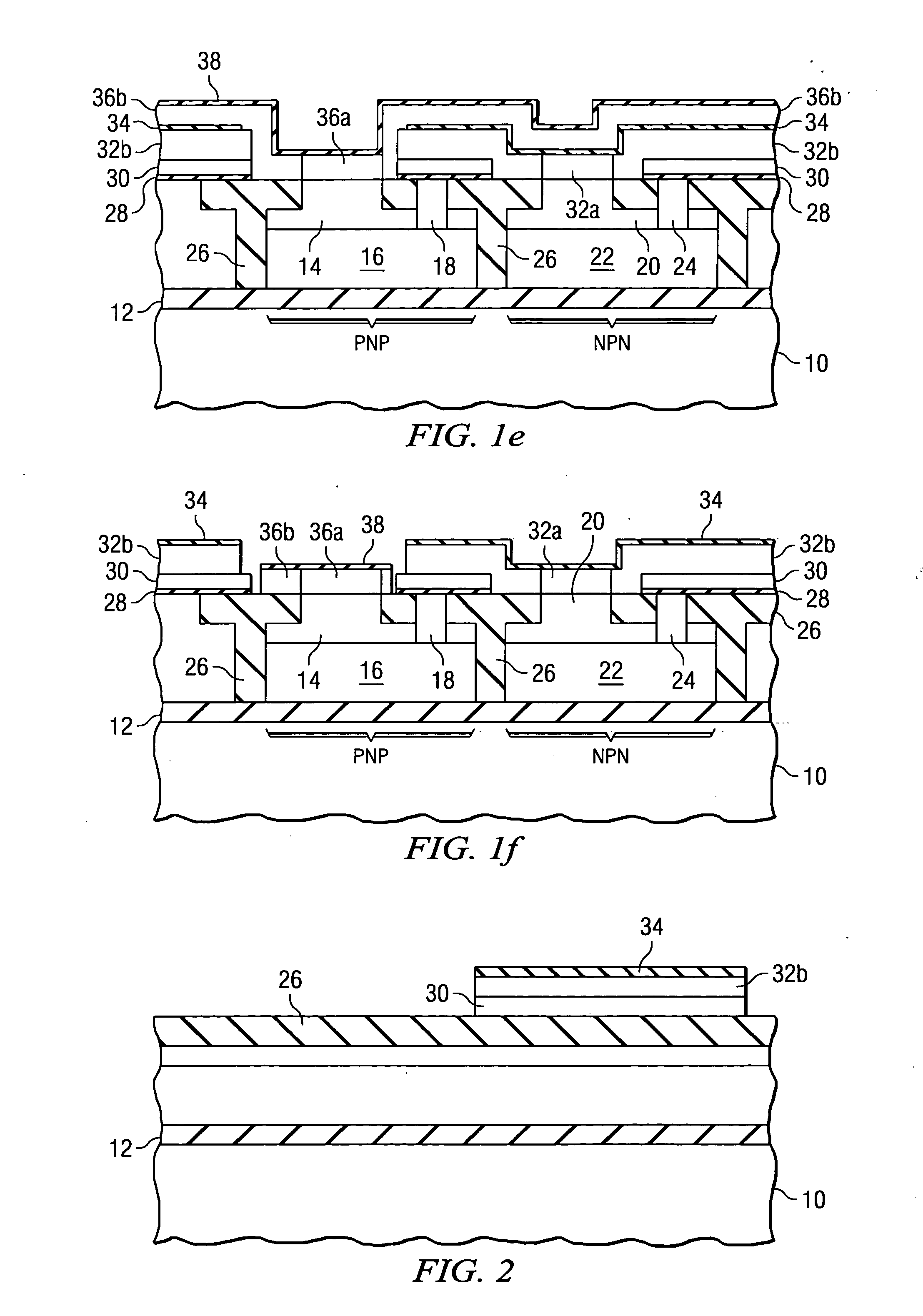
[0012] Referring now to FIG. 1a there is illustrated in a side view a section through a wafer 10 consisting substantially of silicon. Deposited on the wafer 10 are a few structures serving as the starting point for the method in accordance with the invention as detailed in the following. The wafer 10 comprises, running parallel to the top face, a buried layer 12 consisting of silicon dioxide, for example, and used for electrically insulating the overlying layers. Over the buried layer 12 the wafer 10 is provided with two regions formed simultaneously, each of which may form the collector region of a bipolar transistor. In the following the method in accordance with the invention is described for the case that in the left-hand region, termed PNP in FIG. 1a, a bipolar PNP transistor is to be formed whilst in the right-hand region termed NPN in FIG. 1a, a bipolar NPN transistor is formed.

[0013] In the first collector region the collector of an NPN transistor is formed. This region is ...


PUM


Abstract

In a method of fabricating complementary bipolar transistors with SiGe base regions the base regions of the NPN and PNP transistors are formed one after the other over two collector regions 20, 14 by epitaxial deposition of crystalline silicon-germanium layers 32a, 36a. With this method the germanium profile of the SiGe layers can be freely selected for both NPN and PNP transistors in thus enabling complementary transistor performance to be optimized individually. The SiGe layers 32a, 36a can be doped with an n-type or p-type dopant during or after deposition of the silicon-germanium layers 32a, 36a.

Description

FIELD OF THE INVENTION [0001] The invention relates to a method of fabricating complementary bipolar transistors with SiGe base regions in an SiGe-BiCMOS process. BACKGROUND OF THE INVENTION [0002] Submicron structuring in advanced semiconductor processes achieves a high integration density. Submicron structuring by means of advanced lithographic techniques permits fabrication of greatly scaled down CMOS transistors. The achievable bandwidth and the available driver capacity is, however, restricted in CMOS processes. It is particularly for analog circuits requiring a high cutoff frequency that bipolar transistors are preferably employed, fabricated, for example, from gallium arsenide. Gallium arsenide transistors do not permit integration, however, in conventional CMOS processes. This is why more recently process technologies have been developed comprising fast bipolar transistors combinable with advanced CMOS technologies. One of these technologies is the SiGe-BiCMOS technology in ...

Claims


Application Information

Patent Timeline
Patent Type & Authority Applications(United States)
IPC IPC(8): H01L21/331H01L21/8228
CPCH01L29/66242H01L21/82285
Inventor EL-KAREH, BADIHBALSTER, SCOTTSTEINMANN, PHILIPPSCHARNAGL, THOMASSCHIEKOFER, MANFREDWILLIS, CARL
Owner TEXAS INSTR INC
Why Eureka
Try Eureka