Method and device for processing semicounductor wafer

a technology of semi-counductor and processing method, which is applied in the direction of total factory control, programme control, electric programme control, etc., can solve the problems of delicate variation of the thickness of the film formed on the wafer, deviation of the preset temperature of the processing vessel, and most noticeable deviation of the preset temperature, so as to prevent non-uniform inner state and reliable process

Inactive Publication Date: 2005-01-20
TOKYO ELECTRON LTD
View PDF13 Cites 12 Cited by
  • Summary
  • Abstract
  • Description
  • Claims
  • Application Information

AI Technical Summary

Benefits of technology

[0011] It is, therefore, an object of the present invention to provide a method and device for processing a semiconductor wafer, which enables a reliable process by preventing non-uniformity of inner states of a plurality of processing vessels caused by differences in waiting time between the processing vessels, i.e., differences in time between completion of conditionings of the processing vessels and the transfer of the wafers thereinto.

Problems solved by technology

In particular, the different waiting time period cause the temperature of each processing vessel (a temperature of a susceptor installed in each processing vessel or a temperature of each processing vessel affected by radiation of the susceptor) to be delicately changed, so that the temperatures of the processing vessels deviate from preset temperatures.
Thus, there is a problem with the processing results of the respective processing vessels, e.g., the thickness of films formed on a wafer delicately vary.
While sequentially processing a plurality of wafers, such a problem is most noticeable in a first processed wafer.
And during the processing of the first wafer, the environment is considered unstable.

Method used


Image

  • Method and device for processing semicounductor wafer
  • Method and device for processing semicounductor wafer
  • Method and device for processing semicounductor wafer

Examples


modified example

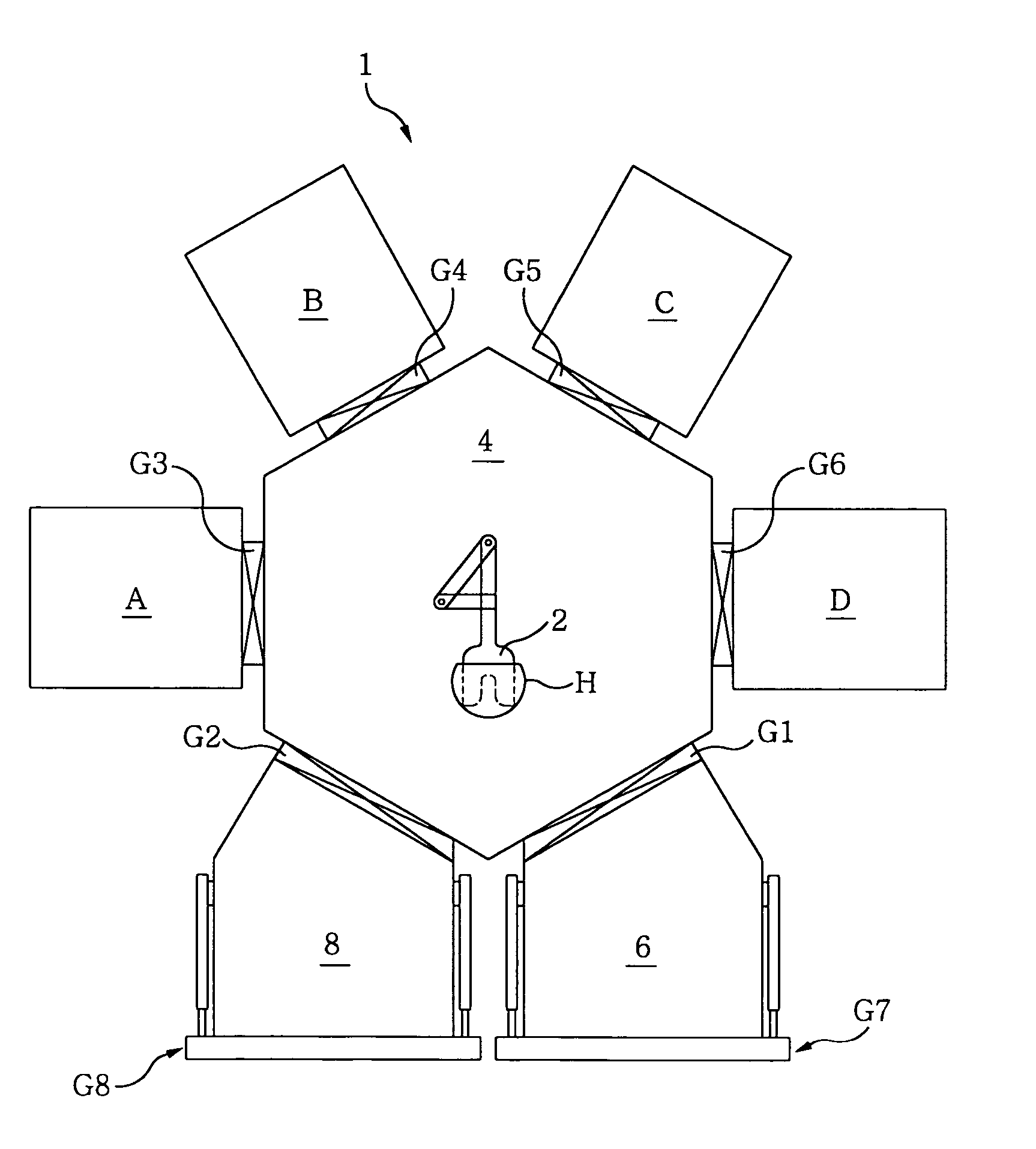
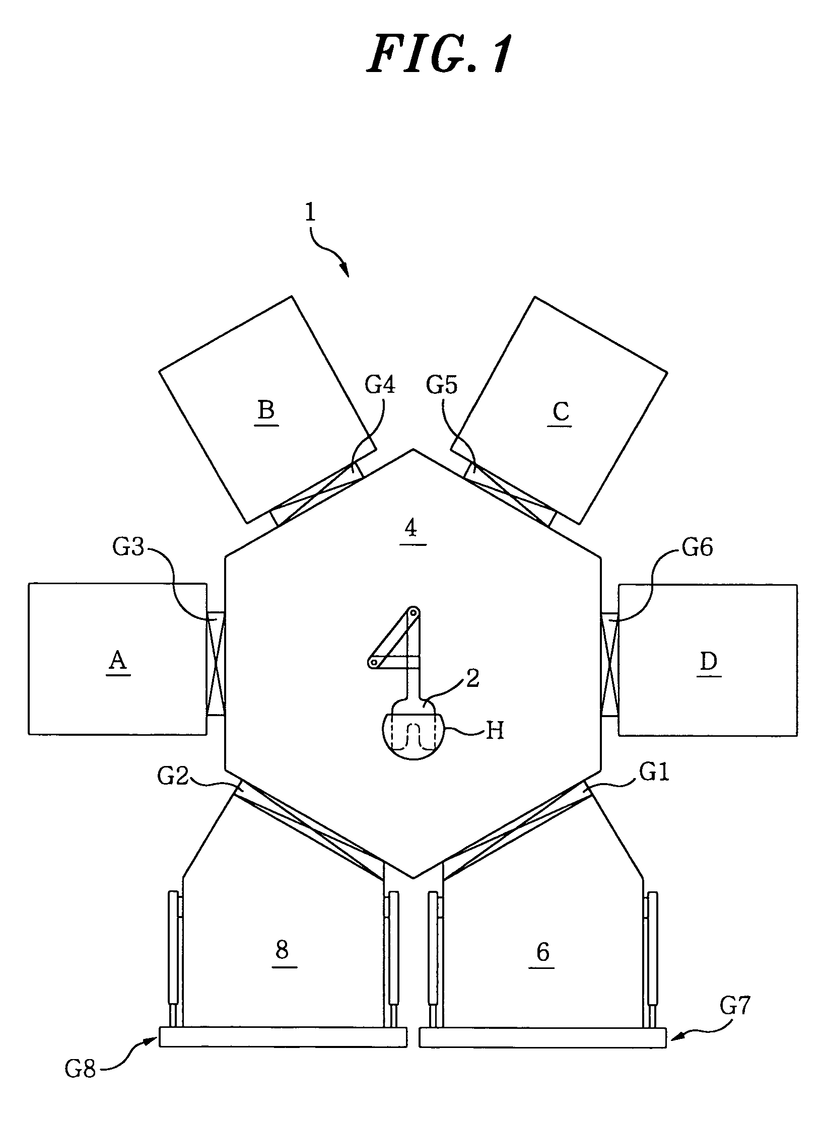
[0077] In the above preferred embodiments, both of the parallel processing and the sequential processing are performed on the premises that the transfer arm 2 is located at the center of the vacuum transfer vessel 4 and, further, the distances between the transfer arm 2 and each of the processing vessels A to D (or X, Y, Z), the load lock chambers 6, 8 are substantially the same. Thus, the transferring times C1 to C4 (or C11 to C13) of the wafer are considered to be almost the same. However, if the transferring time periods are quite different from each other, or if the time intervals between the completion times of the conditionings and the start times of the processes need to be identical to each other, the following method may be used.

[0078] For instance, referring to FIGS. 3 and 4 illustrating the sequential processing, if a maximum value of the different transferring times C1 to C4 is represented by Cmax, C1 to C4 are adjusted such that C1=C2=C3=C4=Cmax. By doing so, the time ...


PUM


Abstract

A method of processing a semiconductor wafer, characterized by comprising the steps of executing a permutation processing for processing (Pi) the semiconductor wafers by using a plurality of processing containers (A, B, C, D) for performing the processings different from each other while sequentially transferring (Ci) the wafers into the processing containers or performing a parallel processing for processing the wafers in the processing containers by using the plurality of processing containers for performing the processings identical to each other and a transfer mechanism used commonly for the processing containers while sequentially transferring the wafers into the processing containers by the transfer mechanism, wherein the processings of the wafers in the processing vessels are performed after the completion of the conditioning (Si) of the processing vessels and, in a first processing, a conditioning start time for a next processing container is adjusted so that the conditioning of the next processing container can be completed when the processing of the previous processing container is completed and, in a second processing, the conditioning start time for the latter processing container is adjusted so that the conditioning of the processing container allowing the wafers to be next transferred therein can be completed when the transfer of the wafers into the processing container is completed.

Description

FIELD OF THE INVENTION [0001] The present invention relates to a method and device for processing a semiconductor wafer by using a plurality of processing vessels for performing processes such as a film formation on the semiconductor wafer. BACKGROUND OF THE INVENTION [0002] In general a processing of semiconductor wafers is carried out by transferring semiconductor wafers into a plurality of processing vessels (chambers) prepared in a processing device by a transfer mechanism. For such processing of semiconductor wafers there are a sequential processing and a parallel processing. The sequential processing is performed by using a plurality of processing vessels each for executing different process, wherein a semiconductor wafer is sequentially transferred through the processing vessels. On the other hand, the parallel processing is performed by using a plurality of processing vessels for carrying out an identical process (e.g., a film formation process) and a transfer mechanism used...

Claims


Application Information

Patent Timeline
Patent Type & Authority Applications(United States)
IPC IPC(8): G05B19/418H01L21/00H01L21/02
CPCG05B19/41865G05B2219/32239H01L21/67276G05B2219/45031G05B2219/32297Y02P90/02H01L21/02
Inventor ARAI, SHINJICHIKUMA, TAKAMASAMOCHIZUKI, MASAHIRO
Owner TOKYO ELECTRON LTD
Why Eureka
Try Eureka