

Ground shield structure
- Summary
- Abstract
- Description
- Claims
- Application Information
AI Technical Summary
Benefits of technology
Problems solved by technology
Method used
Image

Examples
Embodiment Construction
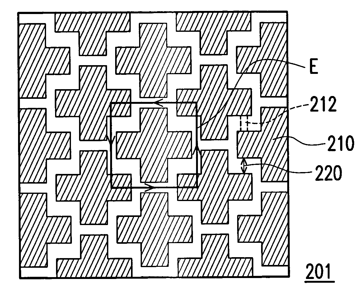
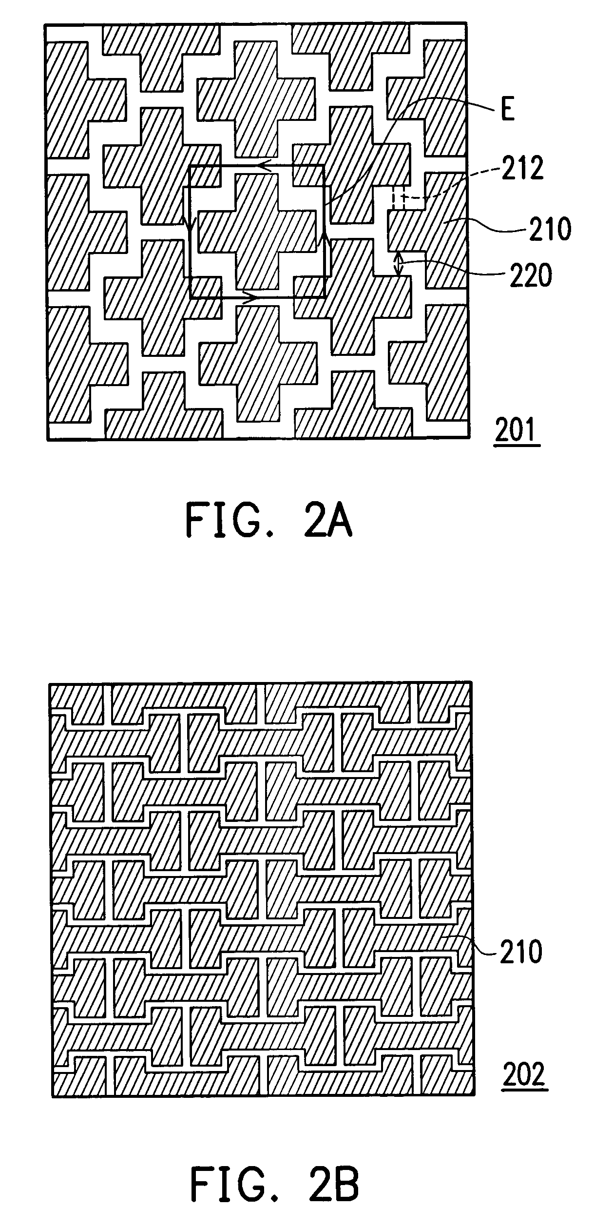
[0019] The ground shield structure of the invention is suitable for use in a circuit structure, such as an integrated circuit, a printed circuit board, a chip package substrate, or other electronic devices, so as to provide the shielding function.
[0020] In FIG. 2A, a ground shield structure is shown, according to the invention. The ground shield structure 201 includes several ground cells 210, with identical profile, like a symbol of “+”. The ground cells 210 are distributed on a ground surface with a periodically and compactly complementary arrangement, wherein a slot 220 exists between two adjacent ground cells 210. It should be noted that the ground surface with the ground cells 210 is not limited to a planar surface. A curved surface is also applicable.
[0021] In addition, in order to electrically connect with the ground cells 210 and allow the ground cells 210 to be able to form a ground shield, the ground shield structure 201 further includes several interconnection members 2...
PUM
 Abstract
Description
Claims
Application Information