Device with n-type semiconductor

a technology of n-type semiconductors and devices, applied in the direction of transistors, solid-state devices, thermoelectric devices, etc., can solve problems such as reducing stability

Inactive Publication Date: 2005-01-27
XEROX CORP
View PDF5 Cites 30 Cited by
  • Summary
  • Abstract
  • Description
  • Claims
  • Application Information

AI Technical Summary

Problems solved by technology

Only a limited number of materials have been developed for the n-type component of such organic complementary circuits, because of the lack of suitable n-type organic materials and theoretical arguments which predict a reduced stability of the n-conducting radical anions under ambient conditions.

Method used


Image

  • Device with n-type semiconductor
  • Device with n-type semiconductor
  • Device with n-type semiconductor

Examples


example 1

Synthesis of BZP (Compound of Formula (12))

About 5.85 grams of 3,4,9,10-perylenetetracarboxylic dianhydride, 26.77 grams of o-phenylene diamine and 7 milliliters of glacial acetic acid were mixed in a round-bottom flask. The resulting mixture was then heated with stirring for 8 hours at 210 degrees C., following by cooling to room temperature. A solid product was then obtained by filtering the mixture through a sintered glass funnel. Then the solid was washed with 1 liter of methanol and slurried with 0.5 liter of 1 percent sodium hydroxide solution. After filtration again, the solid was washed with 600 milliliters of water, and then dried in an oven at 80 degrees C. overnight, yielding 7.5 grams of BZP. The crude product was further purified by sublimation twice for organic TFT use.
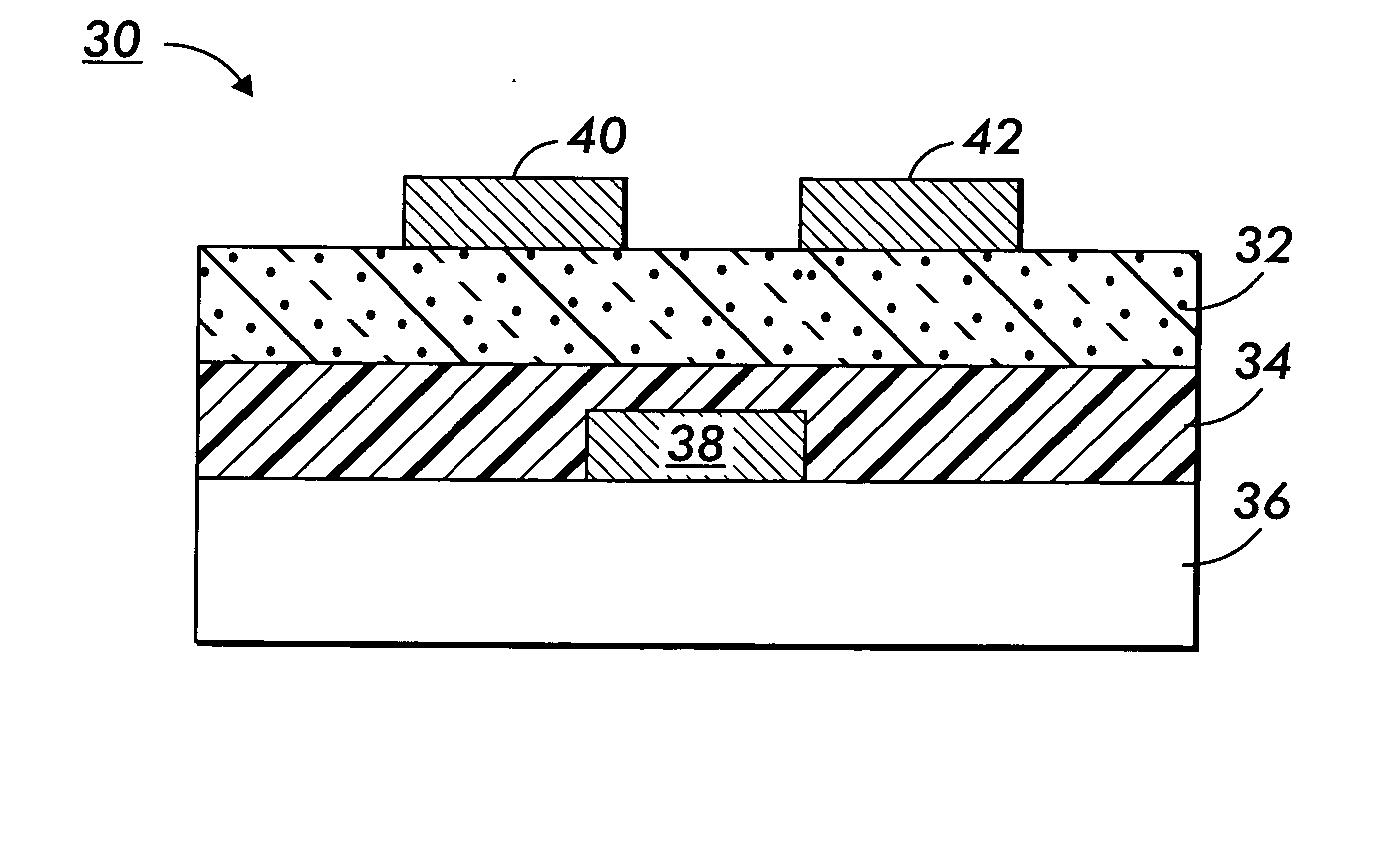
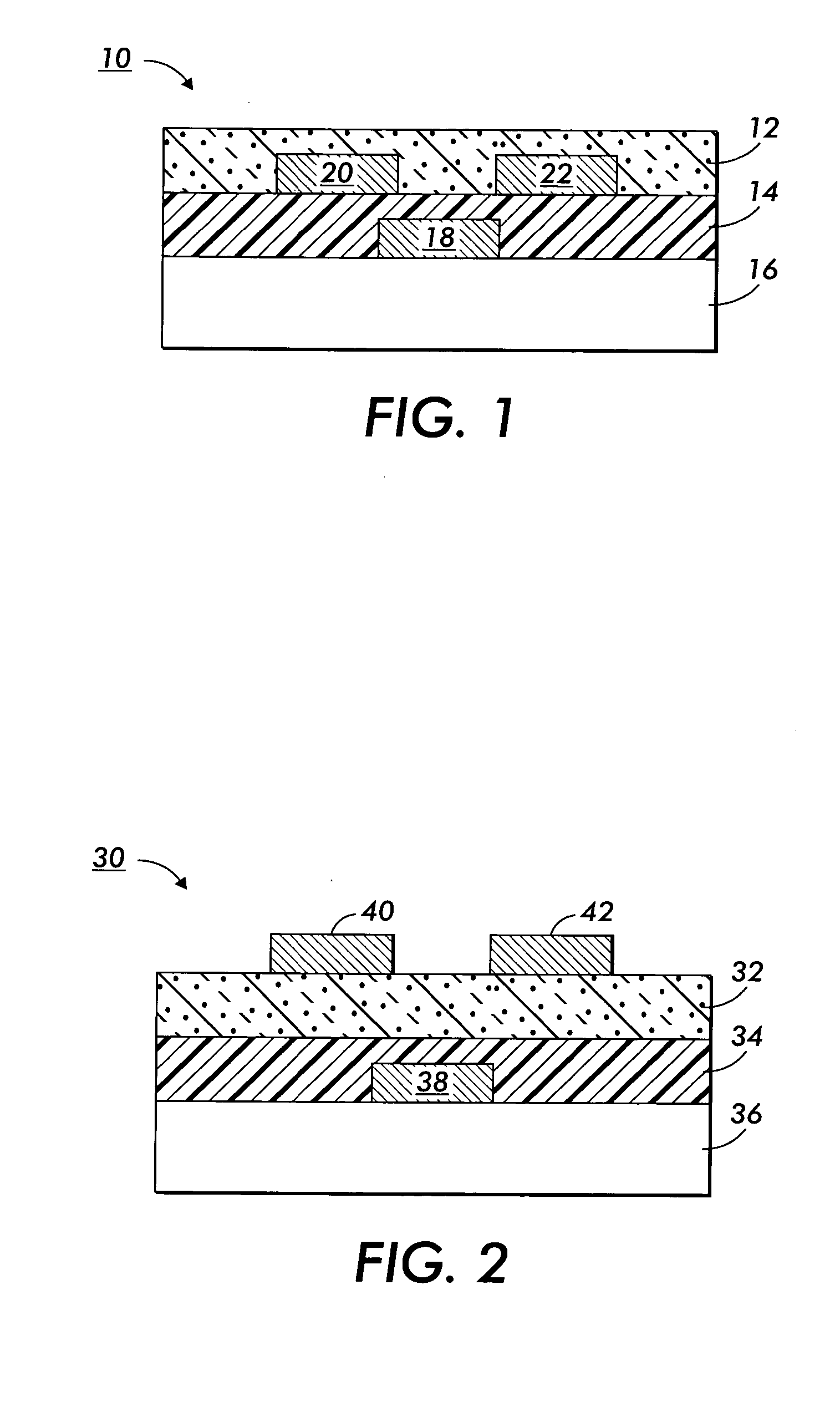
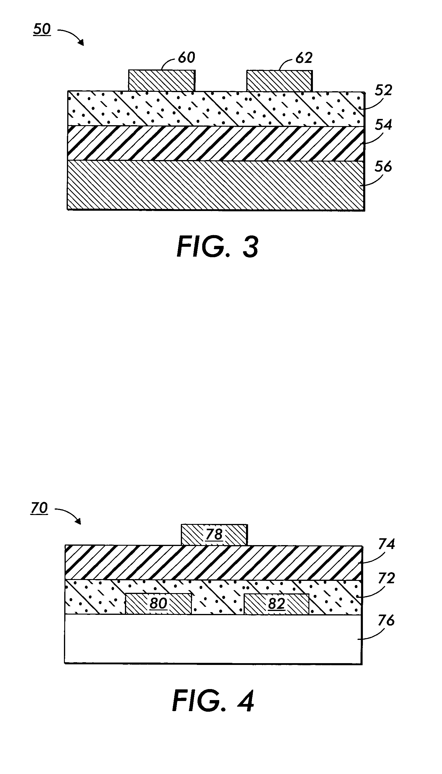
Device Fabrication

There was selected a top-contact thin film transistor configuration as schematically illustrated, for example, in FIG. 3. The test device was comprised of an n-doped silicon wafer ...

example 2

Synthesis of Compound of Formula (19)

About 5.85 grams of 3,4,9,10-perylenetetracarboxylic dianhydride, 18.5 grams of 3,4-diaminotoluene and 7 milliliters of glacial acetic acid were mixed in a round-bottom flask. The resulting mixture was then heated with stirring for 8 hours at 210 degrees C., following by cooling to room temperature. A solid product was then obtained by filtering the mixture through a sintered glass funnel. Then the solid was washed with 1 liter of methanol and slurried with 0.5 liter of 1 percent sodium hydroxide solution. After filtration again, the solid was washed with 600 milliliters of water, and then dried in an oven at 80 degrees C. overnight, yielding 7.8 grams of Compound of Formula (19). The crude product was further purified by sublimation twice for organic TFT use.

example 3 (

HYPOTHETICAL EXAMPLE)

Synthesis of Compound of Formula (8)

About 0.015 mole of 1,4,5,8-naphthalenetetracarboxylic dianhydride, 0.02 mole of o-phenylene diamine and 7 milliliters of glacial acetic acid are mixed in a round-bottom flask. The resulting mixture is then heated with stirring for 8 hours at 210 degrees C., followed by cooling to room temperature. A solid product is then obtained by filtering the mixture through a sintered glass funnel. Then the solid is washed with 1 liter of methanol and slurried with 0.5 liter of 1 percent sodium hydroxide solution. After filtration again, the solid is washed with 600 milliliters of water, and then dried in an oven at 80 degrees C. overnight. The crude product is used for next step reaction.

About 0.01 mole of above product, 0.03 mole of 2,3-naphthalene diamine and 7 milliliters of glacial acetic acid are mixed in a round-bottom flask. The resulting mixture is then heated with stirring for 8 hours at 210 degrees C., following by cooling...


PUM

PropertyMeasurementUnit
thicknessaaaaaaaaaa
thicknessaaaaaaaaaa
thicknessaaaaaaaaaa

Abstract

An electronic device includes a semiconductor layer in contact with a number of electrodes, wherein the semiconductive layer includes a compound wherein either or both of the following geometric isomers of the compound are present: wherein: n is 1, 2 or 3 for the polycyclic moiety; and R1 and R2 are independently selected from the group consisting of a hydrocarbon ring and a heterocyclic group, wherein R1 and R2 are the same or different hydrocarbon ring, the same or different heterocyclic group, or one of R1 and R2 is the hydrocarbon ring and the other the heterocyclic group.

Description

BACKGROUND OF THE INVENTION Thin film transistor (referred herein as “TFT”) is the key component of integrated circuits for electronic devices. Although organic material based TFTs generally provide lower performance characteristics than their conventional silicon counterparts, such as silicon crystal or polysilicon TFTs, they are nonetheless sufficiently useful for applications in areas where high mobility is not required. These include large area devices, such as image sensors, active matrix liquid crystal displays and low-end microelectronics such as smart cards and RFID tags. TFTs fabricated from organic or polymer materials are potentially very low cost, and may also be functionally and structurally more desirable than conventional silicon technology in the aforementioned areas in that they may offer mechanical durability, structural flexibility, compact and light weight characteristics, and the potential of being able to be incorporated directly onto the active media of the d...

Claims


Application Information

Patent Timeline
Patent Type & Authority Applications(United States)
IPC IPC(8): H01L29/786H01L51/05H01L51/30
CPCH01L51/0044H01L51/0545H01L51/0072H01L51/0053H10K85/154H10K85/621H10K85/6572H10K10/466
Inventor ONG, BENG S.MURTI, DASARAO K.DUFF, JAMES M.WU, YILIANG
Owner XEROX CORP
Why Eureka
Try Eureka