Temperature-to-digital converter

a digital converter and temperature measurement technology, applied in the field of integrated circuit design, can solve the problems of low yield of tdcs during the fabrication process, prone to operational variance, and complex circuits that contain high power dissipation in implementations

Inactive Publication Date: 2005-01-27
MICROCHIP TECH INC
View PDF11 Cites 33 Cited by
  • Summary
  • Abstract
  • Description
  • Claims
  • Application Information

AI Technical Summary

Benefits of technology

In one embodiment, a delta-sigma ADC is coupled to a temperature sampling circuit and a voltage sampling circuit, where the temperature sampler circuit includes a first PN-junction coupled directly to the delta-sigma ADC, in effect providing a ΔVBE signal directly to the delta-sigma ADC. An integrator inherent in the delta-sigma ADC may be used to amplify ΔVBE, eliminating the need for a fixed gain amplifier. Amplification provided by the integrator may be used to match the voltage range of ΔVBE, which corresponds to the input dynamic range of the PN-junction over temperature, to the dynamic range of the delta-sigma ADC, which corresponds to the output voltage range of the delta-sigma ADC. The delta-sigma ADC may also perform subtracting an offset voltage from the amplified ΔVBE to compensate for ΔVBE being non-zero at the lowest operating temperature of the PN-junction, thus centering the voltage range of the amplified ΔVBE to the dynamic range of the delta-sigma ADC.

Problems solved by technology

Many digital systems, especially those that include high-performance, high-speed circuits, are prone to operational variances due to temperature effects.
Temperature-to-digital converters (TDC) of such implementations usually contain complex circuits with high power dissipation.
The yield of these TDCs during the fabrication process may also be low as there are many components that need to be matched for a given process spread.
Disadvantages of the typical system as illustrated in FIG. 1 include a need for large capacitors (such as CI and CT) to meet matching requirements for a fixed-gain amplifier.

Method used


Image

  • Temperature-to-digital converter
  • Temperature-to-digital converter
  • Temperature-to-digital converter

Examples


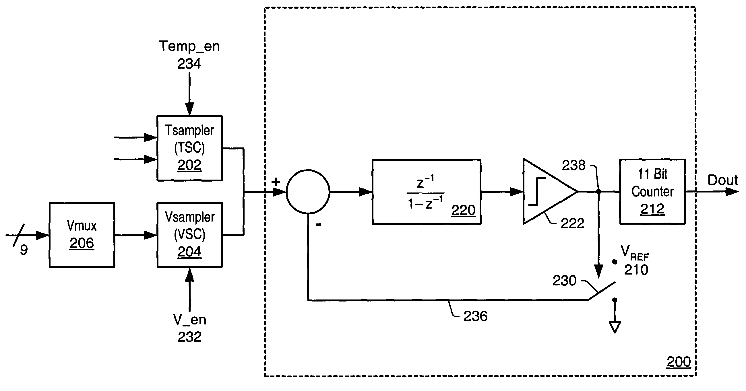
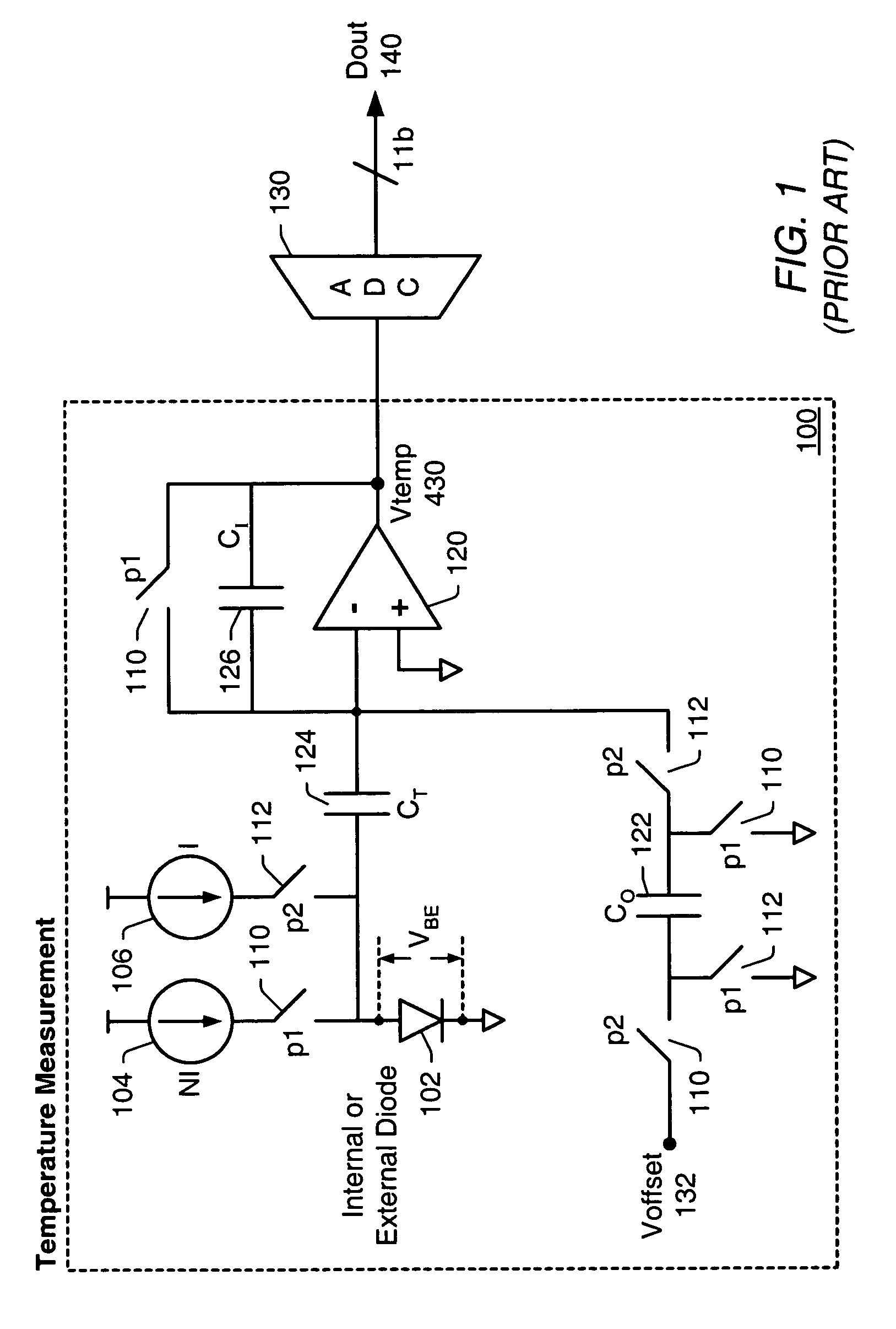
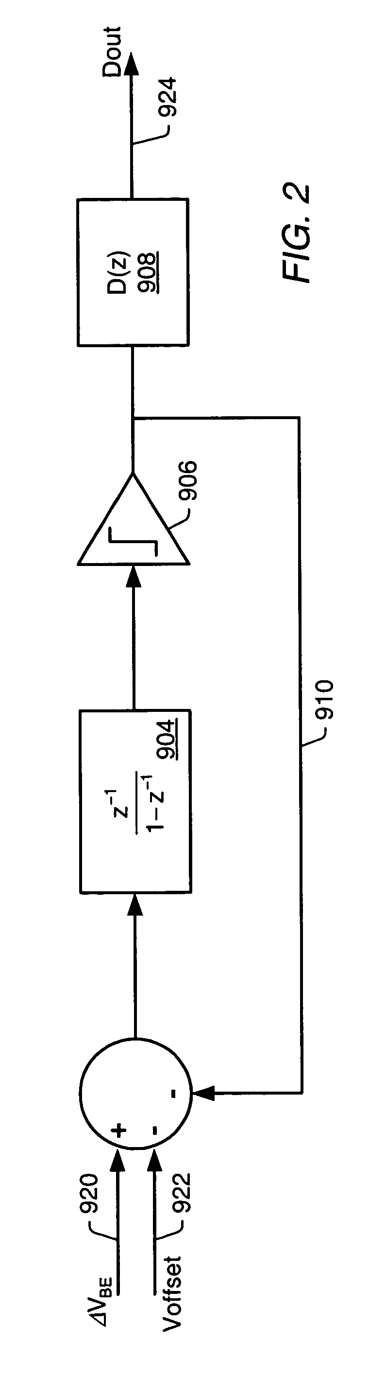
Embodiment Construction

As used herein, a “trigger” signal is defined as a signal that is used to initiate, or “trigger”, an event or a sequence of events in a digital system. A trigger signal is said to be in a “triggering state” at a time when it initiates a desired event, or sequence of events. A periodic trigger signal may commonly be referred to as a “clock”. In a “synchronous” digital system, generally a clock, commonly referred to as a “system clock”, may be used for initiating most events, or sequences of events. An example of a triggering state may be, but is not limited to, a rising edge of a pulse of a clock in a synchronous digital system. A clock is referred to as a “free-running” clock when the clock is available continuously, without interruption, during operations that require the clock. In other words, a clock is not free-running when it is not available during all operations that require the clock.

When an event, or a sequence of events, is said to be initiated “in response to” receivin...


PUM

PropertyMeasurementUnit
temperatureaaaaaaaaaa
voltageaaaaaaaaaa
offset voltageaaaaaaaaaa

Abstract

A temperature to digital converter device is implemented by integrating a temperature sensor circuit into an analog-to-digital converter (ADC). Temperature-to-digital conversion is accomplished by first measuring a change in voltage (ΔVBE) across the junction of a diode when different current densities are forced through the junction. The thus obtained ΔVBE is proportional to temperature. As part of the conversion processing, ΔVBE is multiplied by a fixed gain, and an offset voltage value is subtracted from ΔVBE. The multiplication and subtraction functions are performed by a switched-capacitor integrator in a delta-sigma ADC and the ADC itself operates as the temperature-to-digital converter device, eliminating the extra amplifier and / or capacitors required when the multiplication and / or subtraction function are performed outside the ADC. Alternately, other ADC topologies that include an integrator or gain amplifier, such as pipeline ADCs and cyclic ADCs may be used in place of the delta-sigma ADC.

Description

BACKGROUND OF THE INVENTION 1. Field of the Invention This invention relates generally to the field of integrated circuit design and, more particularly, to the design of temperature measuring devices and analog-to-digital converters in integrated circuit systems. 2. Description of the Related Art Many digital systems, especially those that include high-performance, high-speed circuits, are prone to operational variances due to temperature effects. Devices that monitor temperature and voltage are often included as part of such systems in order to maintain the integrity of the system components. Personal computers (PC), signal processors and high-speed graphics adapters, among others, typically benefit from such temperature monitoring circuits. For example, a central processor unit (CPU) that typically “runs hot” as its operating temperature reaches high levels may require a temperature sensor in the PC to insure that it doesn't malfunction or break due to thermal problems. Often...

Claims


Application Information

Patent Timeline
Patent Type & Authority Applications(United States)
IPC IPC(8): G01K7/01H03M1/06H03M1/34
CPCG01K7/01
Inventor STOCKSTAD, TROY L.
Owner MICROCHIP TECH INC
Why Eureka
Try Eureka