
Nonvolatile semiconductor memory and its test method

Active Publication Date: 2005-01-27
KIOXIA CORP
View PDF4 Cites 27 Cited by
  • Summary
  • Abstract
  • Description
  • Claims
  • Application Information

AI Technical Summary

Benefits of technology

[0043] According to an aspect of the present invention, there is provided a nonvolatile semiconductor memory comprising a memory chip comprising a nonvolatile memory cell array; a write circuit which repeatedly executes a write and a verification on one write unit in the memory cell array to complete a verify write on the write unit; and a write voltage control circuit which changes a write voltage in each write executed repeatedly by the write circuit, the write voltage control circuit comprising: a first binary counter which operates after an initial value for a write voltage has been set, to count a first clock signal supplied every time the verification fails and supply output data to the write circuit as data on a write voltage for each verify write; a first register which stores data for setting the number of writes and verifications on a target write unit; a second binary counter which is reset using a first timing, counts a second clock signal supplied if a verify write executed on the target write unit fails even though the verify write is repeated a number of times set in the first register, and supplies output data to the first binary counter as an initial value for the write voltage; a second register which stores the number of write units used for a test for determining an appropriate value for a write start voltage for the memory chip; an accumulative value storage circuit which is reset using a second timing and stores a value corresponding to an accumulative value for the contents of the second binary counter obtained as a result of the verify write executed on a plurality of write units corresponding to the number of times specified by the second register; and a nonvolatile storage element which stores the appropriate value for the write start voltage for the memory chip in accordance with stored contents of the accumulative value storage circuit and stored contents of the second register.
[0044] According to another aspect of the present invention, there is provided a nonvolatile semiconductor memory comprising a memory chip comprising a nonvolatile memory cell array; an erase circuit which repeatedly executes an erase and a verification on one erase unit in the memory cell array to complete a verify erase on the erase unit; and an erase voltage control circuit which changes an erase voltage in each erase executed repeatedly by the erase circuit, the erase voltage control circuit comprising: a first binary counter which operates after an initial value for an erase voltage has been set, to count a first clock signal supplied every time the verification fails and supply output data to the erase circuit as data on an erase voltage for each verify erase; a first register which stores data for setting the number of erases and verifications on a target erase unit; a second binary counter which is reset using a first timing, counts a second clock signal supplied if a verify erase executed on the target erase unit fails even though the verify erase is repeated a number of times set in the first register, and supplies output data to the first binary counter as an initial value for the erase voltage; a second register which stores the number of erase units used for a test for determining an appropriate value for an erase start voltage for the memory chip; an accumulative value storage circuit which is reset using a second timing and stores a value corresponding to an accumulative value for the contents of the second binary counter obtained as a result of the verify erase executed on a plurality of erase units corresponding to the number of times specified by the second register; and a nonvolatile storage element which stores the appropriate value for the erase start voltage for the memory chip in accordance with stored contents of the accumulative value st

Problems solved by technology

Subsequently, bad columns and rows are detected.
The time required for a wafer test sequence such as the one described above is reflected in the cost of the chip.
This results in a temporal overhead.
However, if the write is started with too low a voltage, a write operation must be repeated a large number of times. This may degrade write performance.
Thus, the initial voltage is not always obtained from a group of memory cells exhibiting a typical write or erase characteristic.
Therefore, disadvantageously, the trimming value is inappropriate for the initial voltage.

Method used


Image

  • Nonvolatile semiconductor memory and its test method
  • Nonvolatile semiconductor memory and its test method
  • Nonvolatile semiconductor memory and its test method

Examples


Embodiment Construction

[0062] An embodiment of the present invention will be described below in detail with reference to the drawings.

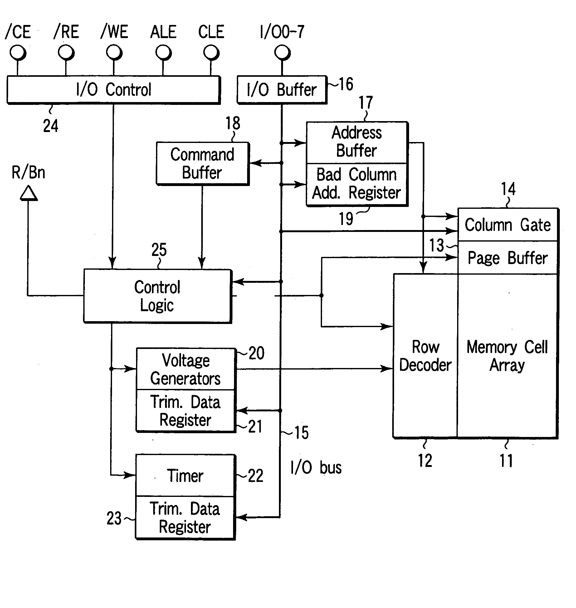
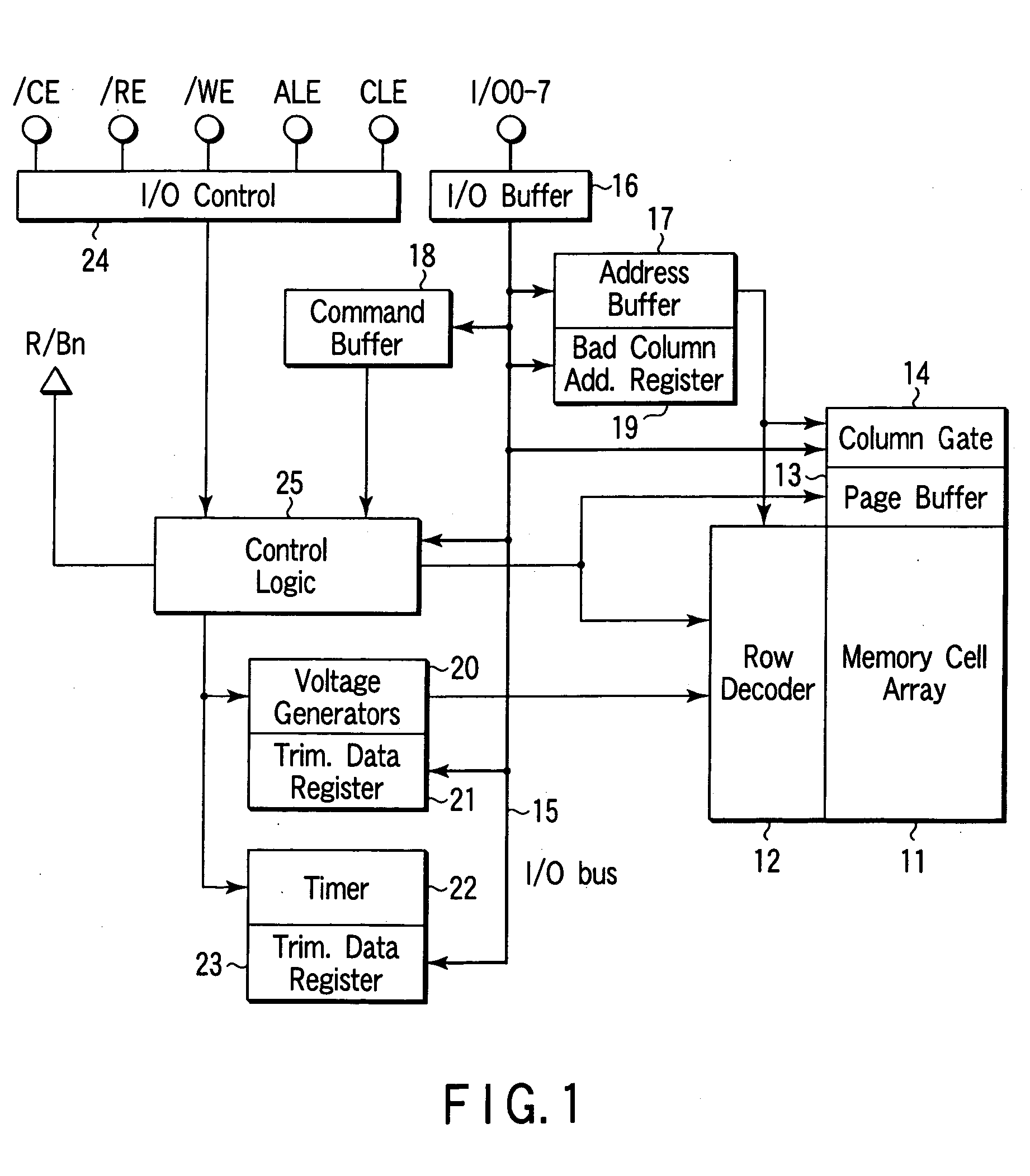
[0063]FIG. 1 is a block diagram showing a block diagram of a NAND type flash memory according to an embodiment of the present invention.

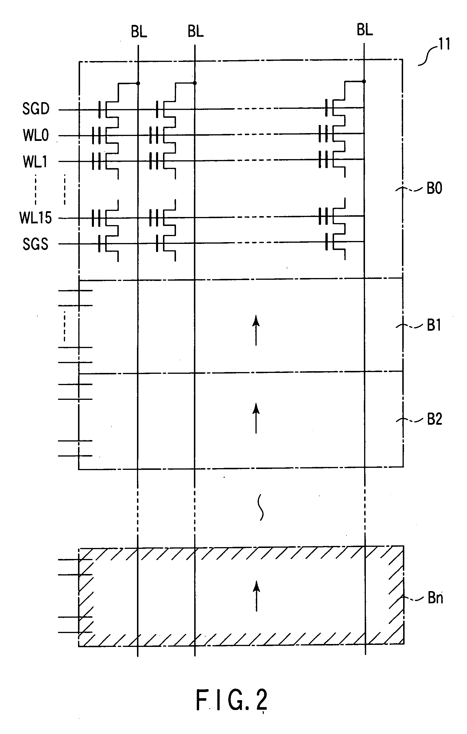
[0064] In FIG. 1, a memory cell array 11 is composed of electrically rewritable nonvolatile memory cells arranged in a column direction and a row direction to form a matrix. Each of the memory cells has a stacked gate type MOS transistor structure in which a control gate and a floating gate are stacked.

[0065] The memory cell array 11 is formed on a well area insulated and separated from the other components. To erase data from a memory cell in the memory cell array 11, the following erase method is employed: an erase operation is divided into a plurality of steps so that an erase voltage applied to the well area is increased in increments of a specified value in each step starting with an initial voltage.

[0066] Further, the memory cell ...


PUM


Abstract

A nonvolatile semiconductor memory is disclosed, which comprises a nonvolatile memory cell array, a write circuit which repeatedly executes a write and a verification, and a write voltage control circuit, the write voltage control circuit comprising a first binary counter which counts a first clock signal supplied every time the verification fails and supplies output data to the write circuit, a first register which stores data for setting the number of erases and verifications, a second binary counter which is reset using a first timing, counts a second clock signal supplied if a verify write executed on the target write unit fails, an accumulative value storage circuit which is reset using a second timing and stores a value corresponding to an accumulative value for the contents of the second binary counter, and a nonvolatile storage element which stores the appropriate value for the write start voltage.

Description

CROSS-REFERENCE TO RELATED APPLICATIONS [0001] This application is a continuation of and claims the benefit of priority under 35 USC §120 from U.S. application Ser. No. 10 / 617,400, filed Jul. 11, 2003 and is based upon and claims the benefit of priority under 35 USC §119 from Japanese Patent Application No. 2002-204442, filed Jul. 12, 2002, the entire contents of which are incorporated herein by reference.BACKGROUND OF THE INVENTION [0002] 1. Field of the Invention [0003] The present invention relates to a nonvolatile semiconductor memory and its test method, and in particular, to a circuit that sets an initial value for a write voltage and an initial value for an erase voltage both of which are used for a nonvolatile semiconductor memory that carries out verify writes and verify erasures, as well as a test method for this circuit. The present invention is applicable to, for example, a NAND type flash memory. [0004] 2. Description of the Related Art [0005] A NAND type flash memory, ...

Claims


Application Information

Patent Timeline
IPC IPC(8): G11C16/00G11C16/02G11C29/44G11C29/50G11C29/56
CPCG11C16/04G11C16/3481G11C29/50004G11C29/12005G11C29/50G11C29/028G11C16/00
Inventor IMAMIYA, KENICHIKAWAI, KOICHI
Owner KIOXIA CORP
Learn More