Non-volatile semiconductor memory device and electric device with the same

a semiconductor memory and non-volatile technology, applied in the direction of digital storage, instruments, transistors, etc., can solve the problems of data processing overhead time, waste of remaining block area, and data rewriting tim

Inactive Publication Date: 2005-01-27
KK TOSHIBA
View PDF5 Cites 51 Cited by
  • Summary
  • Abstract
  • Description
  • Claims
  • Application Information

AI Technical Summary

Problems solved by technology

If only small capacity data is written in such a large block of the NAND-type flash memory, the remaining area of the block becomes wasteful.
However, using the above described erasing scheme in which a block is adapted to a data erase unit, it takes an extra time for data rewriting.
This brings an overhead time in data processing.
However, in the above described selective erase method, there is a problem that the erase-inhibition states in the non-selected area are not uniform, and a large erase stress is applied to a cell adjacent to the selected area.
In other words, one of the non-selected word lines, which is adjacent to a selected word line, is not boosted to a sufficient high voltage.
This results in that the number of erase operations is limited, or such a case may occur that the erase operation becomes impossible.

Method used


Image

  • Non-volatile semiconductor memory device and electric device with the same
  • Non-volatile semiconductor memory device and electric device with the same
  • Non-volatile semiconductor memory device and electric device with the same

Examples


Embodiment Construction

[0032] Illustrative embodiments of this invention will be explained with reference to the accompanying drawings below.

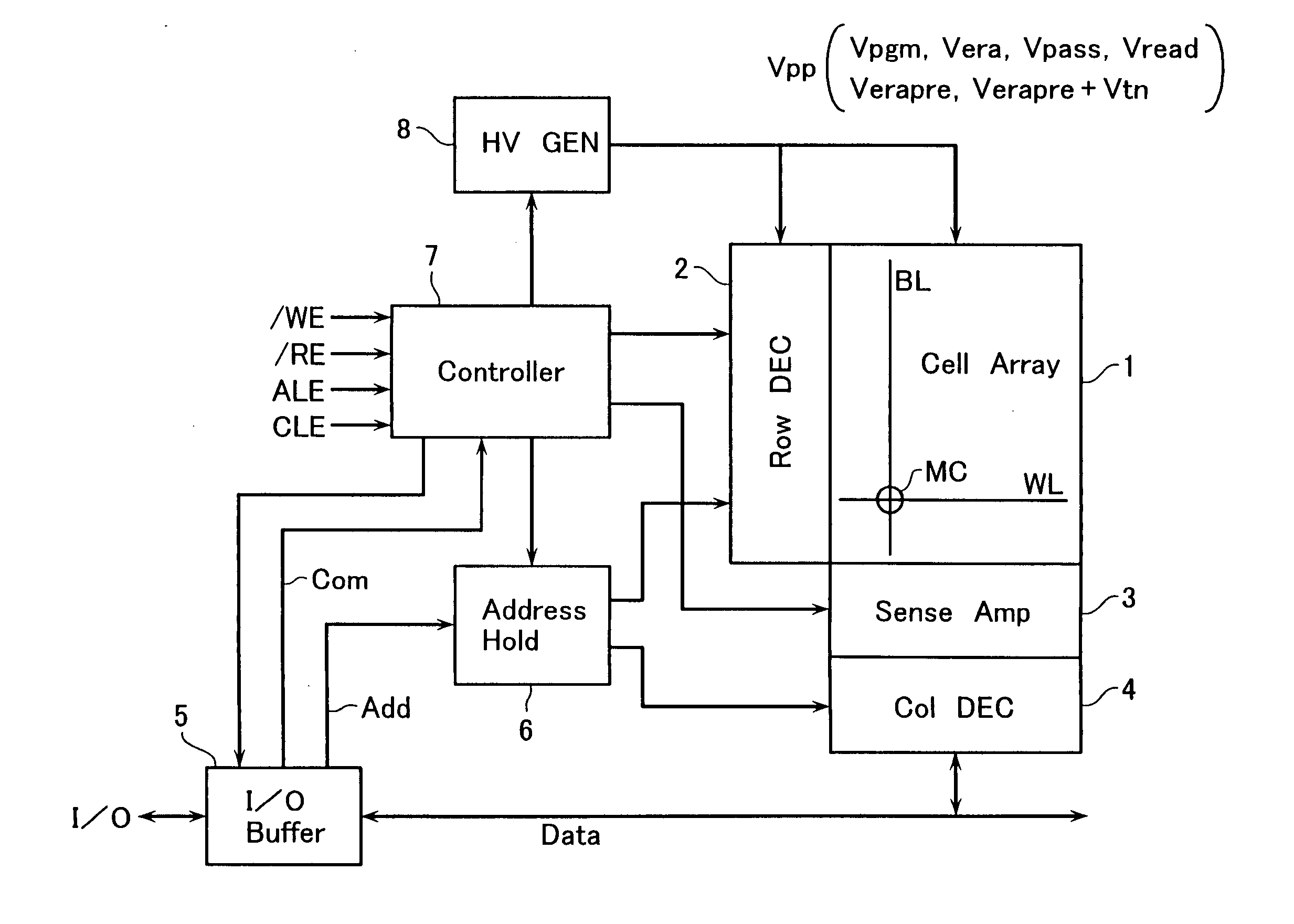
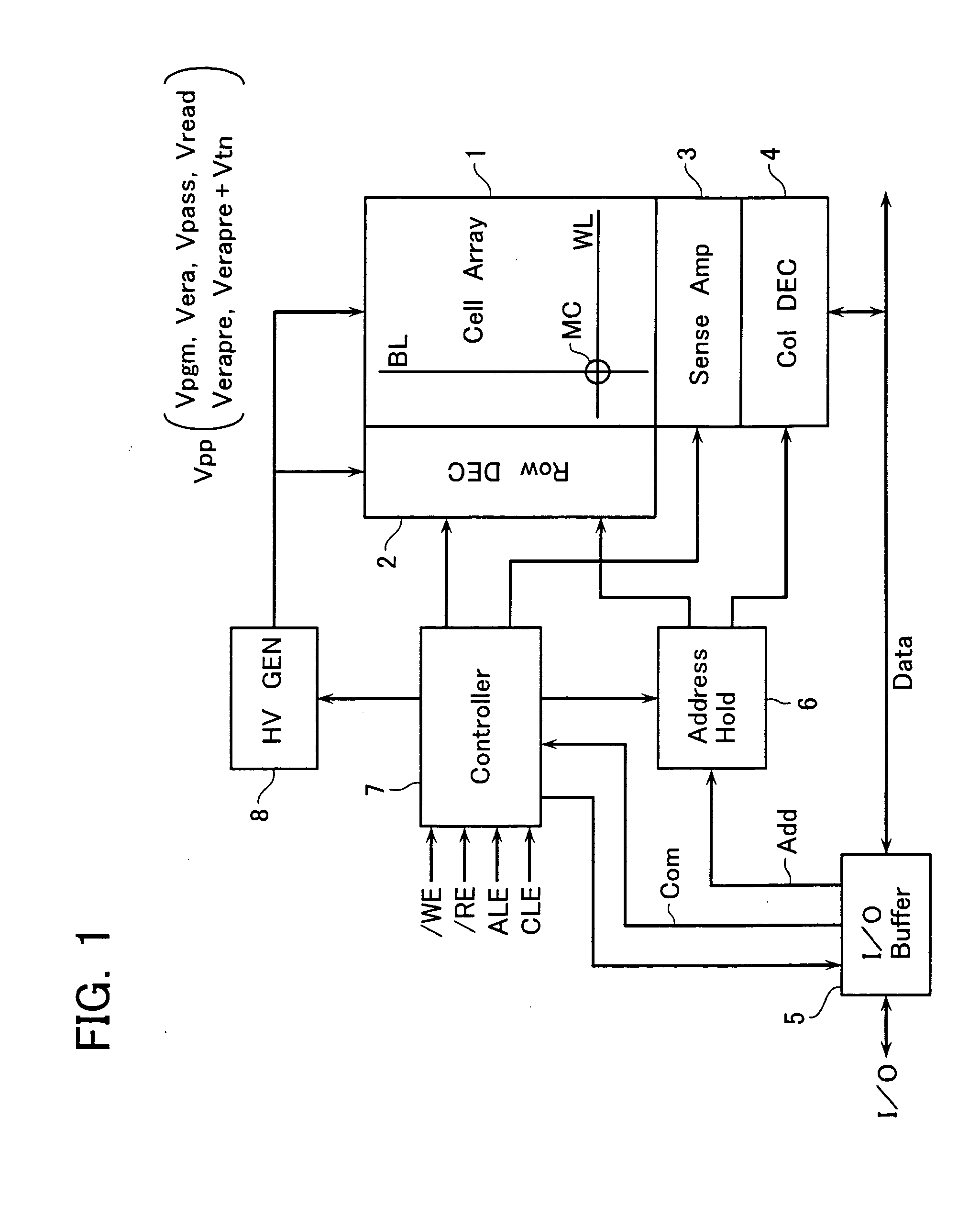
[0033]FIG. 1 shows a functional configuration of a NAND-type flash memory in accordance with an embodiment. Arranging a plurality of floating-gate type memory cells MC in a matrix manner, a cell array 1 is formed. A row decoder circuit (including word line driver) 2 is disposed for driving word lines and select gate lines of the cell array 1. A sense amplifier circuit 3 has sense amplifiers and data latch circuits, and constitutes a page buffer which is used for data writing and reading by a page of the cell array 1.

[0034] One page read data in the sense amplifier circuit 3 may be selected by a column decoder (column gates) 4 to be output to the external I / O terminal through an I / O buffer 5. Write data supplied from the I / O terminal is selected by the column decoder 4 to be loaded in the sense amplifier circuit 3. One page write data is loaded in the sense amplifie...


PUM


Abstract

A non-volatile semiconductor memory device includes: a cell array having electrically rewritable and non-volatile memory cells disposed at the respective intersections of word liens and bit lines intersecting each other; a row decoder circuit for selectively driving a word line of the cell array; a sense amplifier circuit disposed in communication with the cell array for data reading and writing; and a controller for executing sequence control of data write and erase, wherein in a data erase cycle controlled by the controller to erase memory cells disposed along at least one selected word line of the cell array, an adjacent / non-selected word line which is non-selected and adjacent to the selected word line in non-selected words lines in the cell array is precharged to a first erase-inhibition voltage, while the remaining non-selected word lines are precharged to a second erase-inhibition.

Description

CROSS-REFERENCE TO RELATED APPLICATION [0001] This application is based on and claims the benefit of priority from the prior Japanese Patent Application No. 2003-188537, filed on Jun. 30, 2003, the entire contents of which are incorporated herein by reference. BACKGROUND OF THE INVENTION [0002] 1. Field of the Invention [0003] This invention relates to a non-volatile semiconductor memory device and an electric device with the same. [0004] 2. Description of Related Art [0005] Currently known EEPROMs are mostly formed of memory cells floating gates of which store data charge. Arranging NAND cell units each having a plurality of memory cells connected in series, a cell array of a NAND-type flash memory which is known as one of the EEPROMs is constructed. Source and drain diffusion layers of the memory cells in the NAND cell unit are shared with adjacent cells. To increase the capacity of the NAND-type flash memory, it is effective to increase the number of cells in the NAND cell unit, ...

Claims


Application Information

Patent Timeline
Patent Type & Authority Applications(United States)
IPC IPC(8): G11C16/06G11C8/10G11C11/34G11C16/02G11C16/04G11C16/14G11C16/16G11C16/34H01L21/8247H01L27/00H01L27/10H01L27/115H01L29/788H01L29/792
CPCG11C8/10G11C16/0483G11C16/16G11C16/3445G11C16/3427G11C16/344G11C16/3418G11C16/14H01L27/00
Inventor HOSONO, KOJI
Owner KK TOSHIBA
Why Eureka
Try Eureka