Array of non volatile split-gate memory cells for avoiding parasitic programming and programming method thereof

Inactive Publication Date: 2005-01-27
EM MICROELECTRONIC-MARIN
View PDF7 Cites 55 Cited by
  • Summary
  • Abstract
  • Description
  • Claims
  • Application Information

AI Technical Summary

Benefits of technology

[0025] Given this general goal, one particular object of the present invention is to ensure efficient programming of a particular cell using a low supply voltage wit

Problems solved by technology

The combined result of these two effects is a high risk of unwanted or parasitic programming of cells 24 sharing same word control line 18 for a low supply voltage VDD close to programming voltage VPROG.
The problem of such unwanted programming ar

Method used


Image

  • Array of non volatile split-gate memory cells for avoiding parasitic programming and programming method thereof
  • Array of non volatile split-gate memory cells for avoiding parasitic programming and programming method thereof
  • Array of non volatile split-gate memory cells for avoiding parasitic programming and programming method thereof

Examples


first embodiment

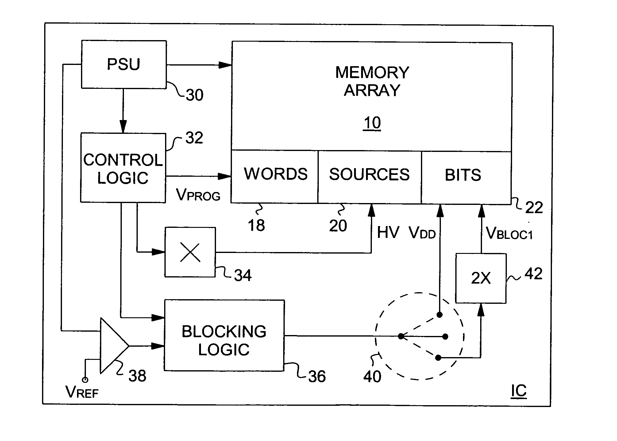
[0045]FIG. 4A shows the integration of a memory array as previously defined into an integrated circuit IC conforming to the invention. The integrated circuit is supplied with power at a low voltage VDD by an external or internal power supply 30. The circuit includes memory array 10 as previously defined, i.e. the memory cells disposed in rows and in columns, plus cell control logic 32 delivering control signals via word control lines 18, source control lines 20 and bit control lines 22, respectively, as well as voltage amplifier means, for example a charge pump 34 for delivering a high voltage HV applied via source control line 20 to the sources of memory cells including a cell that is to be programmed. The circuit further comprises blocking logic 36 for delivering a blocking signal VBLOC1 that may be applied via bit control line 22 to the drains of cells sharing same word control line 18 as a cell that is to be programmed, in accordance with the first programming mode described abo...

second embodiment

[0049] When the second embodiment is used with the first programming mode, there are additionally provided means 38 for comparing supply voltage VDD with the minimum supply voltage or reference voltage VREF required for the integrated circuit IC to operate. If supply voltage VDD is greater than reference voltage VREF, activation means such as a switch 40, for example, are set to supply supply voltage VDD direct to the drains of cells that are not to be programmed but share same word control line 18 as a cell that is to be programmed via bit control line 22 corresponding to those cells. If supply voltage VDD is substantially equal to reference voltage VREF, then activation means 40 are set so that supply voltage VDD is amplified by voltage amplifier means, for example a voltage doubler 42 delivering at its output a blocking voltage VBLOC1 that is greater than supply voltage VDD and is applied via corresponding bit control lines 22 to the drains of cells that are not to be programmed ...


PUM


Abstract

There is disclosed an array (10) of split-gate non-volatile memory cells (24) supplied with power at a low voltage (VDD) by a power supply (30), said cells being arranged in one or more rows and columns and electrically interconnected in groups to form one or more pages (12). The array comprises control logic (32) delivering a defined programming voltage (VPROG) that is close or or substantially equal to the low power supply voltage that is applied to a control gate (245) of at least one cell (24A) that is to be programmed via a word control line (18) corresponding to that cell and blocking logic (36) delivering a first blocking voltage (VBLOC1) that is greater than said low power supply voltage and is applied to the first regions (241) of the cells (24B) sharing the same word control line (18) as said cell that is to be programmed via a bit control line (22) corresponding to those cells.

Description

[0001] This application claims priority from European Patent 03016786.0 filed Jul. 23, 2003, the entire disclosure of which is incorporated herein by reference. TECHNICAL FIELD [0002] The present invention relates generally to an integrated circuit comprising an array of split-gate non-volatile FLASH EEPROM memory cells and using a page architecture for programming and erasing cells. The invention relates more particularly to the use of such memory array architectures for onboard applications in smart cards, where they replace conventional non-volatile memories. [0003] The present invention also relates to a method of programming a memory cell of this kind of array. TECHNOLOGICAL BACKGROUND [0004] Arrays of split-gate non-volatile memory cells arranged in one or more rows and columns and electrically interconnected in groups to form one or more pages are already known in the art. For example, U.S. Pat. No. 6,400,603, incorporated herein by reference, describes an array conforming to...

Claims


Application Information

Patent Timeline
IPC IPC(8): G11C11/34G11C16/04G11C16/10G11C16/34
CPCG11C16/0425G11C16/3418G11C16/10
Inventor MARINELLI, FILIPPONARABECH, NADIA
Owner EM MICROELECTRONIC-MARIN
Why Eureka
Try Eureka