Semiconductor wafer dividing apparatus and semiconductor device manufacturing method

a technology of semiconductor devices and dividing apparatuses, which is applied in the direction of metal working apparatus, manufacturing tools, welding/soldering/cutting articles, etc., can solve the problems of dram degradation, deterioration of element characteristics, and dram to be contaminated

Inactive Publication Date: 2005-02-03
KK TOSHIBA
View PDF31 Cites 46 Cited by
  • Summary
  • Abstract
  • Description
  • Claims
  • Application Information

AI Technical Summary

Benefits of technology

[0013] A semiconductor device manufacturing apparatus according to an aspect of the invention comprises etching equipment which etches a film formed on an element forming surface of a semiconductor wafer, thereby defining a dicing line or a chip-dividing line, damage forming equipment which forms damage layers used as starting points to divide a semiconductor wafer into discrete semiconductor chi

Problems solved by technology

In addition, melted Si is re-crystallized so that adjacent elements will tend to interfere with each other, thereby causing chippings to occur.
Further, there occurs a problem that the element characteristic is deteriorated (for example, the pause characteristic of a DRAM is degraded) or a melted portion is attached to the wiring surface by heat generated at the time of laser application.
Thus, in the conventional semiconductor device manufacturing method and apparatus, when the semiconductor wafer is cut and divided into discrete

Method used


Image

  • Semiconductor wafer dividing apparatus and semiconductor device manufacturing method
  • Semiconductor wafer dividing apparatus and semiconductor device manufacturing method
  • Semiconductor wafer dividing apparatus and semiconductor device manufacturing method

Examples


first embodiment

[0056] [First Embodiment]

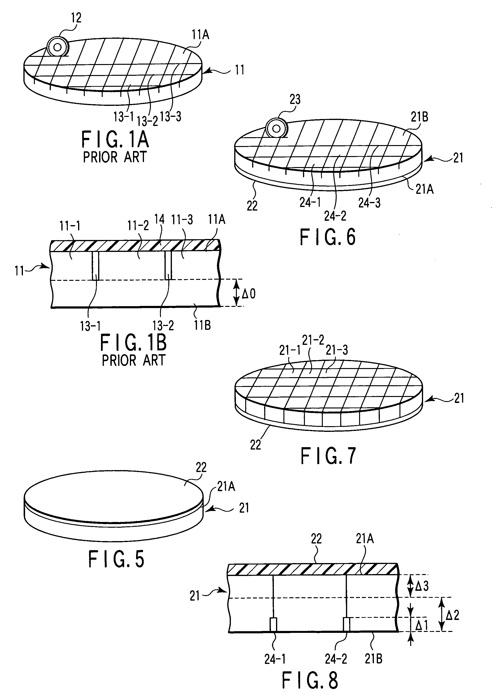
[0057] FIGS. 5 to 9 show parts of a manufacturing process and parts of a manufacturing apparatus, for illustrating a semiconductor device manufacturing method and apparatus according to a first embodiment of the present invention.

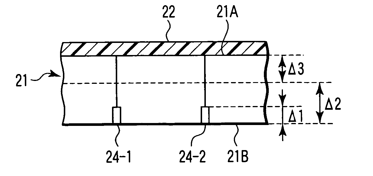
[0058] First, as shown in FIG. 5, a dicing tape (protection member, protection tape or holding tape) 22 is affixed to an element forming surface 21A side of a semiconductor wafer 21 on which elements have been formed.

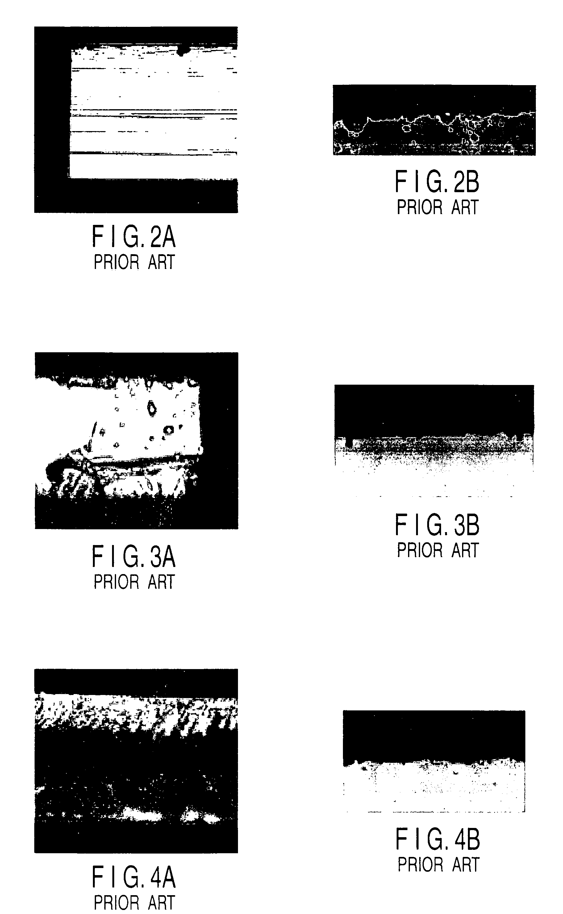
[0059] Next, as shown in FIG. 6, grooves (damage regions or damage layers) 24-1, 24-2, 24-3, . . . used as starting points to divide the semiconductor wafer into discrete semiconductor chips are formed on a rear surface 21B side of the semiconductor wafer 21 which is opposite to the element forming surface 21A by use of a diamond blade 23. The grooves 24-1, 24-2, 24-3, . . . are formed shallower than the thickness of the semiconductor chip obtained at the time of completion. Further, it is preferable to form the groov...

second embodiment

[0066] [Second Embodiment]

[0067] FIGS. 11 to 15 sequentially shows parts of a manufacturing process and parts of a manufacturing apparatus, for illustrating a semiconductor device manufacturing method and apparatus according to a second embodiment of the present invention.

[0068] First, as shown in FIG. 11, a dicing tape (protection member, protection tape or holding tape) 22 is affixed to an element forming surface 21A side of a semiconductor wafer 21 on which elements have been formed.

[0069] Next, as shown in FIG. 12, scratches or distortions (damage regions or damage layers) 28-1, 28-2, 28-3, . . . used as starting points to divide the semiconductor wafer into discrete semiconductor chips are formed on a rear surface 21B side of the semiconductor wafer 21 which is opposite to the element forming surface 21A by use of a diamond scriber 27. The scratches or distortions 28-1, 28-2, 28-3, . . . are formed shallower than the thickness of the semiconductor chip obtained at the time of...

third embodiment

[0076] [Third Embodiment]

[0077] FIGS. 16 to 20 show parts of a manufacturing process and parts of a manufacturing apparatus, for illustrating a semiconductor device manufacturing method and apparatus according to a third embodiment of the present invention.

[0078] First, as shown in FIG. 16, a dicing tape (protection member, protection tape or holding tape) 22 is affixed to an element forming surface 21A side of a semiconductor wafer 21 on which elements have been formed.

[0079] Next, as shown in FIG. 17, Si re-crystallization layers (damage layers or damage regions) 30-1, 30-2, 30-3, . . . used as starting points to divide the semiconductor wafer into discrete semiconductor chips are formed on a rear surface 21B side of the semi-conductor wafer 21 which is opposite to the element forming surface 21A by irradiating a laser beam from a laser irradiation device 29. The re-crystallization layers 30-1, 30-2, 30-3, . . . are formed shallower than the thickness of the semiconductor chip o...


PUM

PropertyMeasurementUnit
Thicknessaaaaaaaaaa
Depthaaaaaaaaaa
Crystallization enthalpyaaaaaaaaaa

Abstract

A semiconductor device manufacturing apparatus includes etching equipment, damage forming equipment, dividing equipment and removing equipment. The etching equipment etches a film formed on an element forming surface of a semiconductor wafer, thereby defining a dicing line or a chip-dividing line. The damage forming equipment forms damage layers used as starting points to divide a semiconductor wafer into discrete semiconductor chips on a rear surface side of the semiconductor wafer which is opposite to an element forming surface. The dividing equipment divides the semiconductor wafer into discrete semiconductor chips with the damage layers used as the starting points. The removing equipment removes a rear surface portion of the semiconductor wafer to at least a depth where the damage layers are no more present.

Description

CROSS-REFERENCE TO RELATED APPLICATIONS [0001] This is a Continuation-in-Part application of U.S. patent application Ser. No. 10 / 390,900, filed Mar. 19, 2003, the entire contents of which are incorporated herein by reference. [0002] This application is based upon and claims the benefit of priority from prior Japanese Patent Applications No. 2003-004767, filed Jan. 10, 2003; and No. 2004-005549, filed Jan. 13, 2004, the entire contents of both of which are incorporated herein by reference.BACKGROUND OF THE INVENTION [0003] 1. Field of the Invention [0004] This invention relates to a semiconductor device manufacturing method and apparatus to discretely divide a semiconductor wafer into semiconductor chips (semiconductor elements) after elements are formed in the semiconductor wafer and more particularly to a technique for discretely dividing the semiconductor wafer. [0005] 2. Description of the Related Art [0006] Conventionally, when a semiconductor wafer on which elements have been f...

Claims


Application Information

Patent Timeline
IPC IPC(8): B23K26/38B23K26/40B28D5/00H01L21/00
CPCB23K26/4075H01L21/67092B28D5/0011B23K2201/40B23K26/40B23K2101/40B23K2103/50
Inventor TAKYU, SHINYAKUROSAWA, TETSUYASATO, NINAO
Owner KK TOSHIBA
Why Eureka
Try Eureka