Method for the fabrication of isolation structures
a technology of isolation structure and manufacturing method, which is applied in the direction of basic electric elements, electrical equipment, and semiconductor devices, etc., can solve the problems of misalignment problems with the underlying structure, the condition for manufacturing insulating structure becomes more critical, and the drawback is much more eviden
- Summary
- Abstract
- Description
- Claims
- Application Information
AI Technical Summary
Benefits of technology
Problems solved by technology
Method used
Image
Examples
first embodiment
[0043] The figures representing cross sections of portions of an integrated circuit during the manufacturing are not drawn to scale. They are instead drawn to show the important features of the invention. With reference to FIGS. 25 to 30, the method for manufacturing insulating structures according to the invention, particularly of the STI type, is described. For convenience of illustration, elements being structurally and functionally similar to the prior art will be given the same reference numerals.
[0044] A first insulating layer 2, for example a very thin oxide layer, being about 10 nm thick, is formed on a semiconductor substrate 1, whereon a stopping layer 3 is formed, for example a silicon nitride layer, being traditionally 100-200 nm thick. The stopping layer 3 serves as a barrier for the following planarization treatments, while the insulating layer 2 is used as a buffer since the stopping layer 3 and the semiconductor substrate 1 generally have a very different network pit...
second embodiment
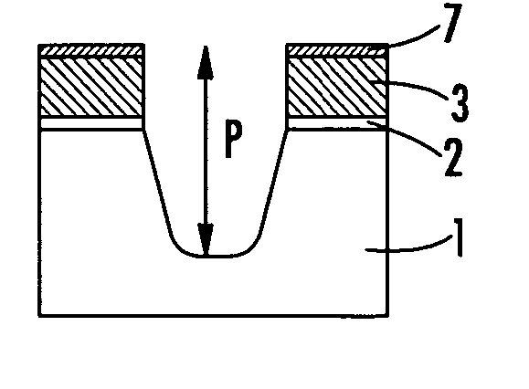
[0056] the method for removing the semiconductor material hard mask 8 provides the same process steps of the previous embodiment until the selective removal of the nitride layer 3, then the methods continues with a semiconductor layer 8 etching step. This etching step is highly selective with respect to oxide and nitride. Afterwards, this latter etching step is followed by a very short removal step of the layer 2 to expose the semiconductor substrate 1 and preserve the second insulating layer 7 on the nitride layer 3. Then it continues with the trench 5 etching, as shown in FIG. 32.
[0057] An important advantage offered by the polysilicon hard mask 8 is given by the possibility to form lower-sized openings 9 with respect to photolithographic ones. In particular, with reference to FIGS. 34 to 39, an alternative embodiment of the method according to the invention is described, wherein a supplementary layer 10, for example a BARC layer, is formed between the resist layer 4 and the semic...
PUM
 Abstract
Description
Claims
Application Information


