Deep reactive ion etching

a reactive ion and etching technology, applied in the direction of decorative surface effects, electrical equipment, decorative arts, etc., can solve the problems of large scallop dimensions, unwanted sidewall roughness, non-uniformity across the wafer, etc., to prevent the growth of roughness, reduce the time to completely remove the deposition in the next deposition removal step, and improve the effect of etching quality

Inactive Publication Date: 2009-10-01
DALSA SEMICON INC
View PDF7 Cites 32 Cited by
  • Summary
  • Abstract
  • Description
  • Claims
  • Application Information

AI Technical Summary

Benefits of technology

[0032]The longer the time of etch at high pressure, the rougher is the bottom surface. The addition of a new step during the etch cycle at low pressure and at high platen power (for efficient ion bombardment) smoothes the bottom of the cavity. This leaves a flat surface prior to the next deposition in the following cycle and prevents the growth of roughness from cycle to cycle. Also, because the deposition is deposited on a flat surface, the time to remove completely the deposition in the next deposition removal step is reduced. This allows higher pressure without roughness on the bottom. Actually, the pressure where the maximum etch rate is obtained can be used with minimal roughness. Because the deposition removal step is reduced, this further increases the etch rate and minimizes attack on the sidewalls.
[0033]An important advantage of this technique is that by using this extra step, the limitation at high pressure is minimized. This gives smoother sidewall and bottom features at fast etch rates. Furthermore, by limiting the non-uniformity on the etch rate across the wafer because of the roughness, embodiments of this invention result in a reduction on the depth non-uniformity across the wafer.
[0034]The Radio Frequency (RF) coil matching network unit needs to be able to react to the fast change of plasma conditions. Reducing the pressure rapidly corresponds to a fast change in impedance and therefore the matching network unit needs to react fast on such changes. The addition of an extra bombardment step reduces the mask selectivity.

Problems solved by technology

This also generates non-uniformities across the wafer because the roughness is rarely uniform across the wafer.
This roughness also causes unwanted sidewall roughness.
All the above steps generally result in larger scallop dimensions.
However, they cause the following disadvantages:a. Larger roughness on the bottom of the etched feature.
After many cycles, this can become dramatic and cause the well known DRIE defect called “grass”.
At one point in time, the vertical roughness defect will grow if it is not removed after each cycle.
This reduces the efficiency of the bombardment but increases its density.
During the beginning of each etch cycle; this is increasing the time needed to remove the deposition of the preceding deposition cycle, causing wall etching (wall breakage) and roughness on the bottom of the etched feature.
As can be observed, when using the 3-Step Method at high pressure, as the cycles are added, the roughness in the bottom of the etched feature gets worse and worse.

Method used


Image

  • Deep reactive ion etching
  • Deep reactive ion etching
  • Deep reactive ion etching

Examples


Embodiment Construction

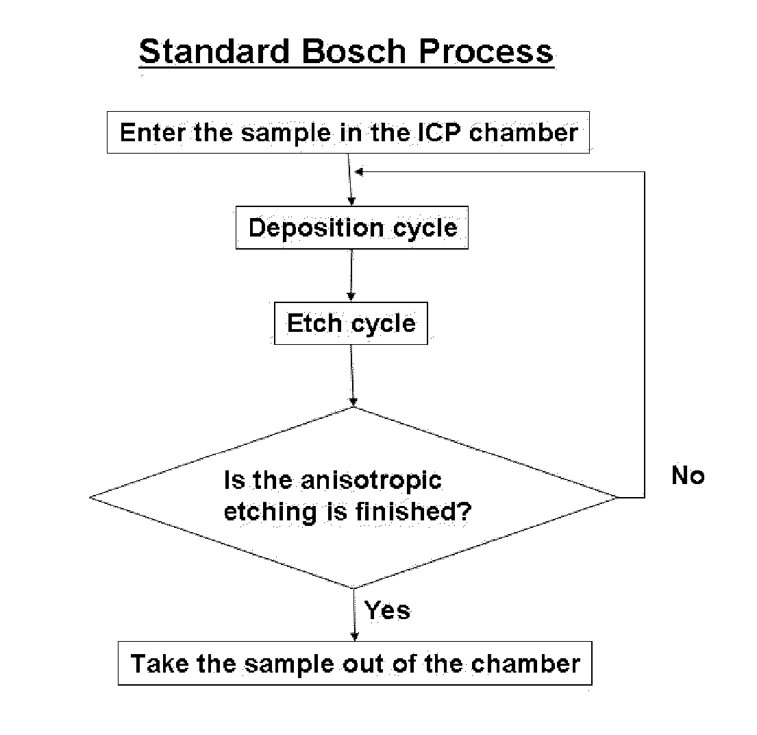
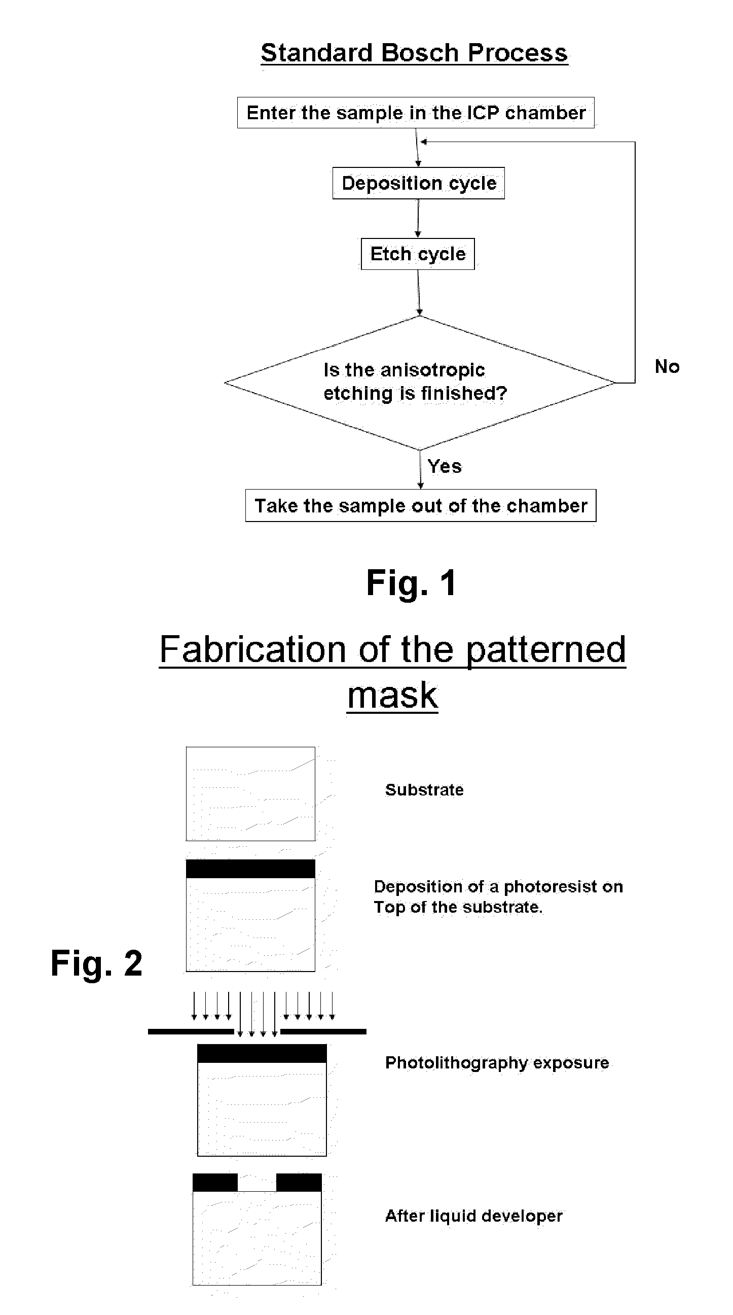
[0062]FIG. 11 shows a sequence diagram in accordance with an embodiment of the present invention. After the substrate has been patterned with a photoresist mask, such as depicted in FIG. 2 or by any other technique, the sample is placed in the ICP chamber. After being clamped on the platen (or chuck) and the process conditions have been stabilized in flow and pressure, the plasma is then lit, and the sample undergoes a deposition, followed by the etching step that removes the deposition. Next, comes a high pressure etching (main etch) as in the 3-step process shown in FIG. 7. Finally, the cycle finishes with another bombardment condition at low pressure and high platen power prior to the next cycle, making a total of four steps per cycle. These four steps are repeated until the right depth is obtained or an underneath etch stop layer is reached.

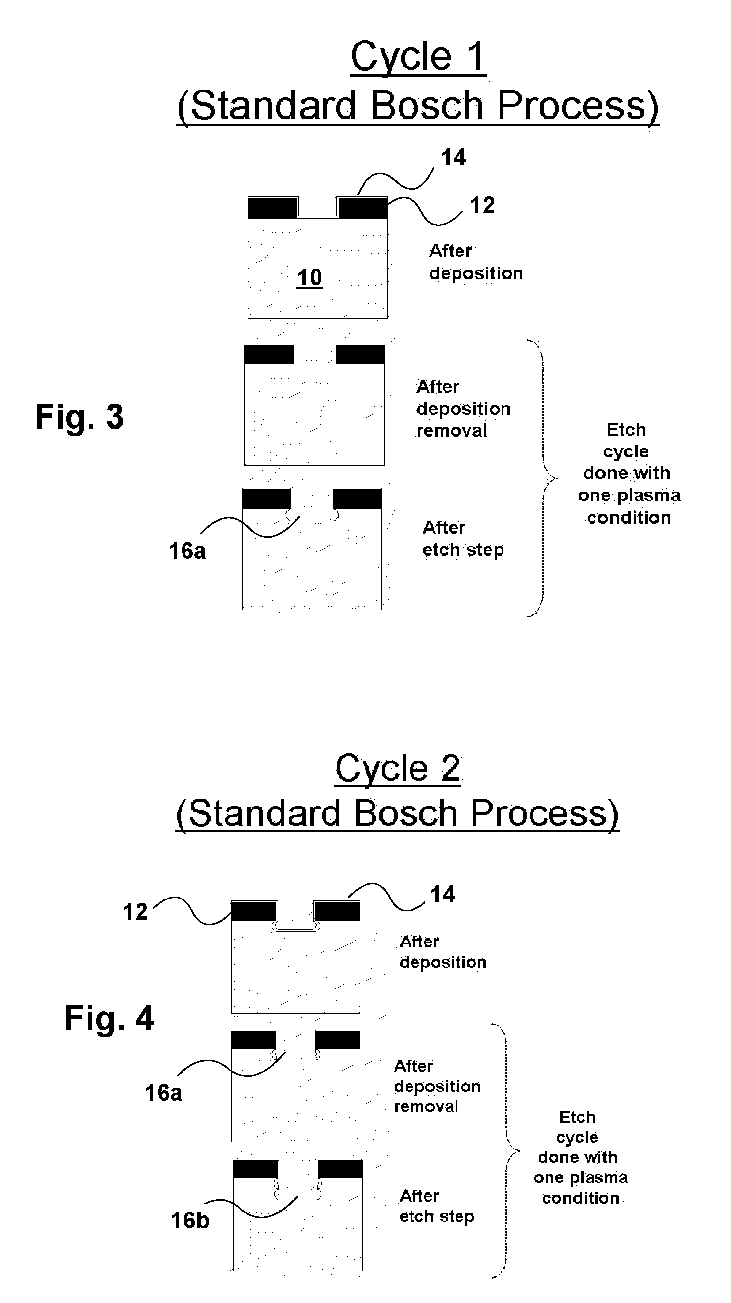
[0063]FIG. 12 is a schematic representation of the steps that the sample encounters during the first cycle of the sequence shown in FIG. 11....


PUM

PropertyMeasurementUnit
pressureaaaaaaaaaa
pressureaaaaaaaaaa
pressureaaaaaaaaaa

Abstract

In a method of performing an anisotropic etch on a substrate in an inductively coupled plasma etch chamber, at least three cycles of a procedure consisting essentially of the four following steps are performed:
    • a. depositing a protective polymer on a patterned substrate;
    • b. performing a first low pressure etch to partially remove the deposited protective polymer at a pressure less than 40 mTorr;
    • c. performing a high pressure etch at a pressure between between 40 mT and 1000 mT to form a portion of a trench in the substrate; and
    • d. performing a second low pressure etch at a pressure less than 40 MTorr to reduce surface roughness.
This method permits the fabrication of deep trenches with reduced surface roughness.

Description

CROSS REFERENCE TO RELATED APPLICATION [0001]This application claims priority under 35 USC 119(e) of U.S. Provisional Application No. 61 / 039,912, filed Mar. 27, 2008, the contents of which are herein incorporated by reference.FIELD OF THE INVENTION [0002]This invention relates to anisotropic etching of substrates, and in particular deep reactive ion etching.BACKGROUND OF THE INVENTION [0003]The so-called “Bosch Process” described in U.S. Pat. Nos. 5,501,893 and 6,127,273, the contents of which are herein incorporated by reference, is for anisotropic etching. This process uses a patterned mask deposited on top of the substrate. The mask needs to be selective to the etching chemistry used for etching the substrate. Then, in an Inductively Coupled Plasma (ICP) system, two plasma conditions are alternated between deposition phase and etching phase. The deposition is done using a gas that deposits a Teflon-like polymer (normally C4F8 is used) and the etching is normally performed using a...

Claims


Application Information

Patent Timeline
Patent Type & Authority Applications(United States)
IPC IPC(8): B44C1/22
CPCH01L21/30655
Inventor BEAUDRY, RICHARD
Owner DALSA SEMICON INC
Why Eureka
Try Eureka