Porous polyurethane polishing pads

Active Publication Date: 2005-02-03
ROHM & HAAS ELECTRONICS MATERIALS CMP HLDG INC
View PDF6 Cites 28 Cited by
  • Summary
  • Abstract
  • Description
  • Claims
  • Application Information

AI Technical Summary

Benefits of technology

[0014] The invention provides a porous polishing pad useful for polishing semiconductor substrates, the porous polishing pad having a porous matrix formed from a coagulated polyurethane and a non-fibrous polishing layer, the non-fibrous polishing layer having a polishing surface with a pore count of at least 500 pores per mm2, the pore count decreasing with removal of the polishing layer and the polishing surface having a surface roughness Ra between 0.01 and 3 μm.
[0015] In addition, the invention provides a method of preparing a porous polishing pad formed from a coagulated polyurethane, the porous polishing pad b

Problems solved by technology

For example, small pores make the pad short-lived because dross and spent slurry tend to clog the pores or get stuck in the underlying cells.
Further, small pores can make it difficult to keep slurry flowing in and out of the cells.
The dross can also become impacted in the cell

Method used


Image

  • Porous polyurethane polishing pads
  • Porous polyurethane polishing pads
  • Porous polyurethane polishing pads

Examples


example

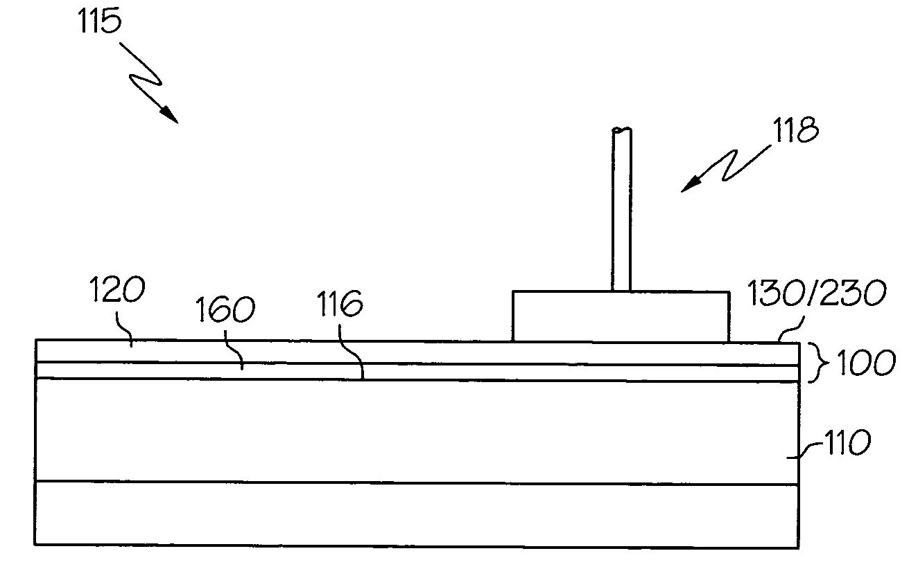
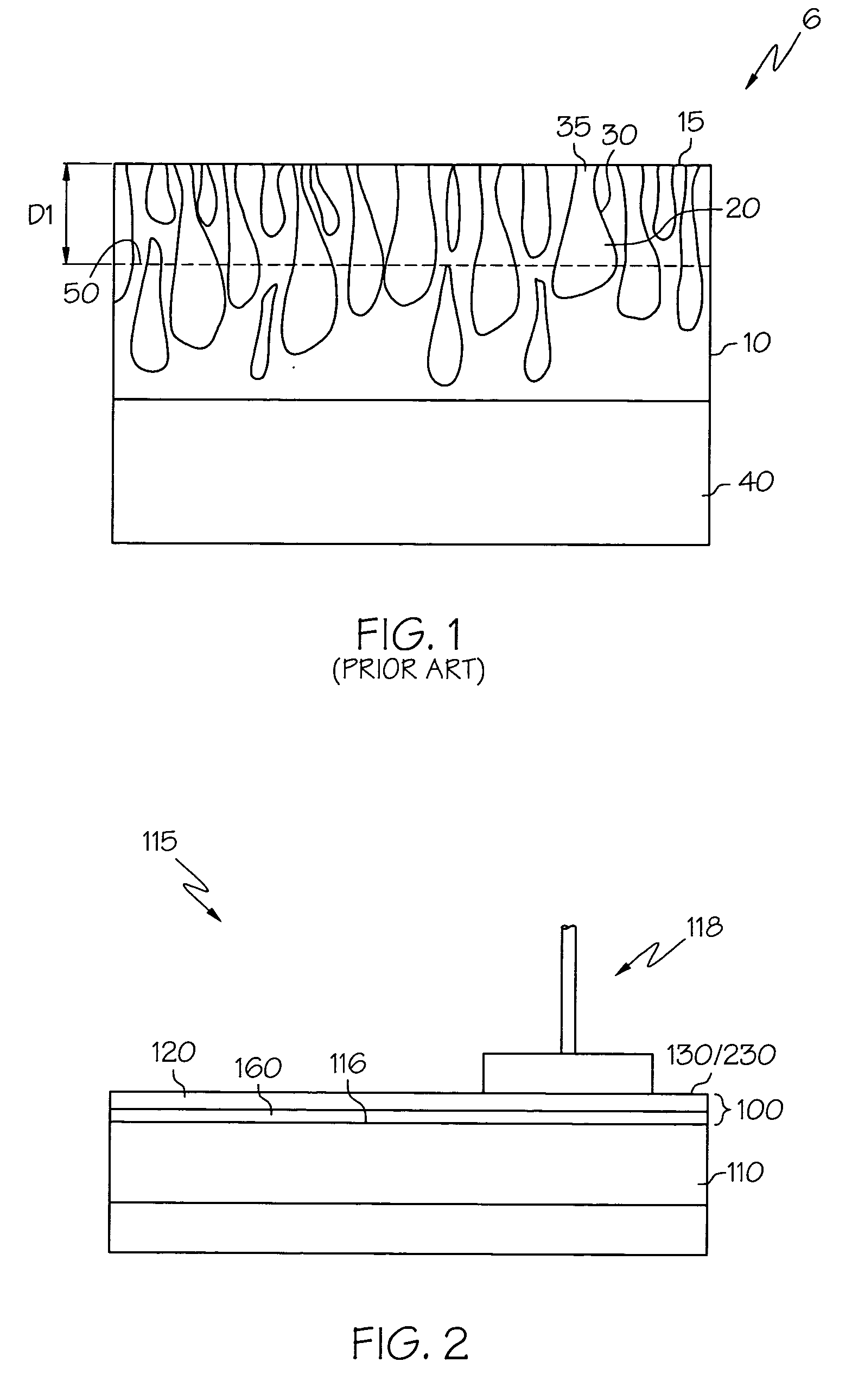
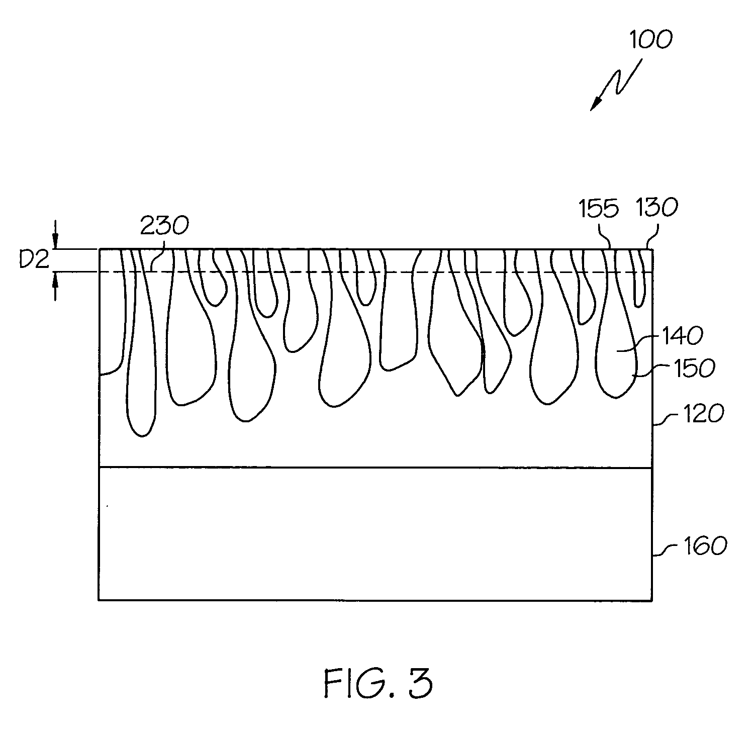
[0032] Comparative examples A, B and C represent porous polishing pads produced by coagulating polyurethane and sanding off the top layer with a belt sanding device—these pads represent commercially available POLITEX™ high, regular and low nap height polishing pads sold by Rodel, Inc. POLITEX™ polishing pads and the polishing pad of the example were porous-non-fibrous polishing pads produced by coagulating polyurethane; and in particular, coagulating a polyetherurethane polymer with polyvinyl chloride produces these pads.

[0033] The following example 1 represents the process used to prepare polishing pads from the non-sanded polishing material of the comparative examples to have a unique combination of high pore count and excellent surface roughness. First, cleaning the platen with isopropyl alcohol prepared the polishing platen. Then mounting the pad to the cleaned polishing platen with minimal trapped air prepared the blank pad for machining. Then cutting the pad on the platen usi...


PUM

PropertyMeasurementUnit
Lengthaaaaaaaaaa
Lengthaaaaaaaaaa
Surface roughnessaaaaaaaaaa

Abstract

A porous polishing pad is useful for polishing semiconductor substrates. The porous polishing pad has a porous matrix formed from a coagulated polyurethane and a non-fibrous polishing layer. The non-fibrous polishing layer has a polishing surface with a pore count of at least 500 pores per mm2 that decreases with removal of the polishing layer; and the polishing surface has a surface roughness Ra between 0.01 and 3 μm.

Description

BACKGROUND OF THE INVENTION [0001] The present invention relates to porous polyurethane polishing pads useful for polishing semiconductor substrates and a method of using the polishing pad. In addition, it relates to a method for forming the porous polishing pads. [0002] In recent years, the requirements for integrated circuit fabrication and the drive toward ever higher circuit densities have made it critical that the surfaces of integrated circuit substrates (e.g., silicon wafers) and magnetic substrates (e.g., nickel-plated disks for memory applications) be polished to increasingly higher degrees of smoothness. The present state of the art for achieving the smoothest surface involves polishing the substrate using a polishing solution and a polishing pad. [0003] One polishing technique for achieving a highly polished surface involves using a porous polishing pad in combination with a polishing slurry or reactive liquid. The porous polishing pad must be firm enough to provide the n...

Claims


Application Information

Patent Timeline
IPC IPC(8): B24B37/24B24D3/10B24D3/32H01L21/304
CPCB24B37/24Y10S451/921B24D3/32B24D3/10
Inventor FAWCETT, CLYDE A.CRKVENAC, T. TODDPRYGON, KENNETH A.FOSTER, BERNARD
Owner ROHM & HAAS ELECTRONICS MATERIALS CMP HLDG INC
Why Eureka
Try Eureka