Semiconductor device having superlattice semiconductor layer and method of manufacturing the same

a semiconductor layer and semiconductor technology, applied in semiconductor devices, lasers, semiconductor lasers, etc., can solve the problems of increasing the driving voltage of the ld, reducing the lifespan of the ld, and the method met the limitation of optimizing the superlattice, so as to reduce the series resistance without reducing the optical confinement

Active Publication Date: 2005-02-10
SAMSUNG ELECTRONICS CO LTD
View PDF5 Cites 24 Cited by
  • Summary
  • Abstract
  • Description
  • Claims
  • Application Information

AI Technical Summary

Benefits of technology

[0010] The present invention provides a semiconductor device having a superlattice semiconductor layer for...

Problems solved by technology

However, AlGaN having a large amount of Al increases a series resistance of the LD that causes an increase in a driving voltage of the LD.
In addition, the increase in the driving voltage of the LD reduces the lifespan of the LD.
However, such a method met th...

Method used


Image

  • Semiconductor device having superlattice semiconductor layer and method of manufacturing the same
  • Semiconductor device having superlattice semiconductor layer and method of manufacturing the same
  • Semiconductor device having superlattice semiconductor layer and method of manufacturing the same

Examples


Embodiment Construction

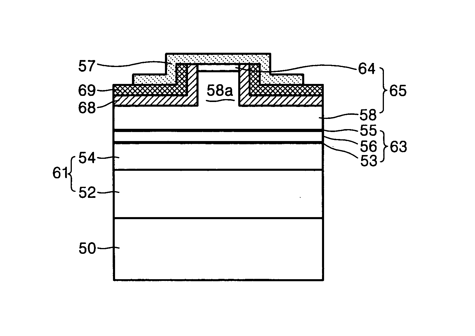
[0028] The present invention will now be described more fully with reference to the accompanying drawings, in which exemplary embodiments of the invention are shown. In the drawings, the thicknesses of layers and regions are exaggerated for clarity.

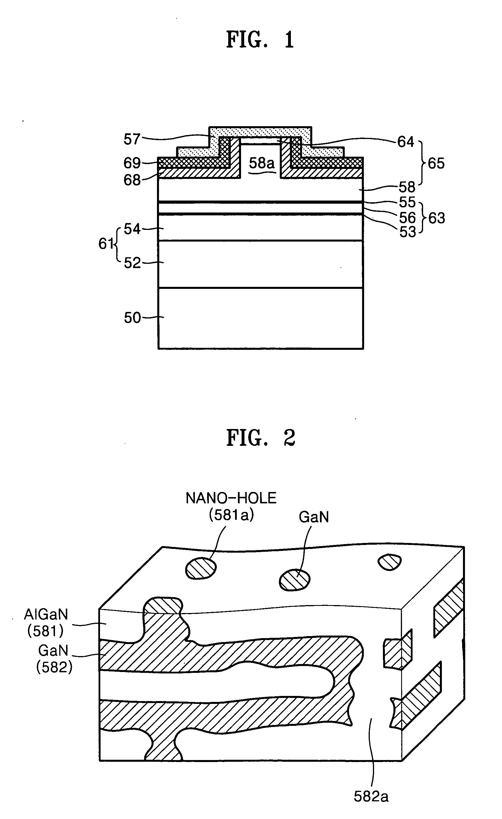
[0029]FIG. 1 is a sectional view illustrating a semiconductor laser diode (LD) according to the present invention. Referring to FIG. 1, a semiconductor LD according to the present invention includes a substrate 50 and a first semiconductor layer 61, a laser resonance layer 62, and a second semiconductor layer 63, which are grown on the substrate 50.

[0030] The first semiconductor layer 61 as a lower material layer includes a buffer layer 52, which is grown on the substrate 50, and a lower cladding layer 54 stacked on the buffer layer 52.

[0031] A sapphire substrate or a free-standing gallium nitride (GaN) substrate is used for the substrate 50. The buffer layer 52 is an n-GaN based group III-V nitride compound semiconductor layer, and it...


PUM


Abstract

Provided are a semiconductor device having a superlattice semiconductor layer and a method of fabricating the same. The semiconductor device includes a superlattice semiconductor layer in which first material layers and second material layers formed of different materials are alternately stacked. A plurality holes are formed in the first material layers and the second material layers forming a superlattice structure, and the holes are filled with materials of the adjacent material layers. The provided superlattice structure reduces a driving voltage by transferring charges through the holes in the first material layers and the second material layers while maintaining a predetermined optical confinement characteristic.

Description

BACKGROUND OF THE INVENTION [0001] This application claims the priority of Korean Patent Application No. 2003-53889, filed on Aug. 4, 2003, in the Korean Intellectual Property Office, which is incorporated herein in its entirety by reference. [0002] 1. Field of the Invention [0003] The present invention relates to a semiconductor having a superlattice semiconductor layer and a method of manufacturing the same, and more particularly, to a semiconductor device having a GaN superlattice semiconductor layer for reducing a driving voltage by decreasing a series resistance and a method of manufacturing the same. [0004] 2. Description of the Related Art [0005] A laser diode (LD) has a superlattice structure in which different materials are stacked to form a multi-layer. For example, a GaN based LD has a superlattice structure in which AlGaN and GaN are stacked in a sandwich structure as shown in FIG. 1. Such a GaN based LD requires AlGaN having a large amount of Al in order to improve an o...

Claims


Application Information

Patent Timeline
IPC IPC(8): H01S5/343B82Y20/00H01L29/15H01L29/20H01S3/0941H01S5/22H01S5/223H01S5/32H01S5/323
CPCB82Y20/00H01L29/155H01L29/2003H01S2301/173H01L33/06H01L33/32H01L33/04H01S3/0941B82Y40/00
Inventor LEE, WON-SEOKHA, KYOUNG-HOKWAK, JOON-SEOPPAEK, HO-SUNLEE, SUNG-NAMSAKONG, TAN
Owner SAMSUNG ELECTRONICS CO LTD
Why Eureka
Try Eureka