Clocked barrier virtual phase charge coupled device image sensor

a virtual phase charge coupled and image sensor technology, applied in the field of solid state image sensors, can solve the problems of generating a small amount of clocking induced spurious charge dark current, smear, and generating smear, and achieves the effects of reducing clocking induced dark current generation, reducing smear, and high performan

Inactive Publication Date: 2005-02-10
TEXAS INSTR INC
View PDF15 Cites 30 Cited by
  • Summary
  • Abstract
  • Description
  • Claims
  • Application Information

AI Technical Summary

Benefits of technology

[0003] It is an object of the present invention to overcome limitations in prior art. It is further object of the present invention to provide a practical image sensor design that minimizes smear and to provide architectures that significantly reduce the generation of clocking induced dark current. It is yet another object of the present invention to provide practical high performance image sensor designs with low spurious charge generation also in the serial and charge multiplication registers. Incorporating the clocked barrier pixel architecture into the image sensing area and the memory area pixels and using the two-phase gate structure accomplishes this task and other objects of the invention.

Problems solved by technology

The FT image sensors, however, have a problem of smear.
This causes generation and collection of unwanted charge in transported pixels that contaminates charge that is being transferred and thus creates smear.
While the VP technology has significant advantages in using fewer clock lines for charge transport and in having high Quantum Efficiency (QE), it has a problem of generating a small amount of clock induced spurious charge dark current.
This becomes a disadvantage in designs that utilize charge multiplication to increase the sensor sensitivity and to reduce noise.
This significantly limits the sensor performance in low light level applications.
While the device cooling may reduce the normal dark current generation, the spurious clock induced dark current actually increases with lowering temperature.

Method used


Image

  • Clocked barrier virtual phase charge coupled device image sensor
  • Clocked barrier virtual phase charge coupled device image sensor
  • Clocked barrier virtual phase charge coupled device image sensor

Examples


Embodiment Construction

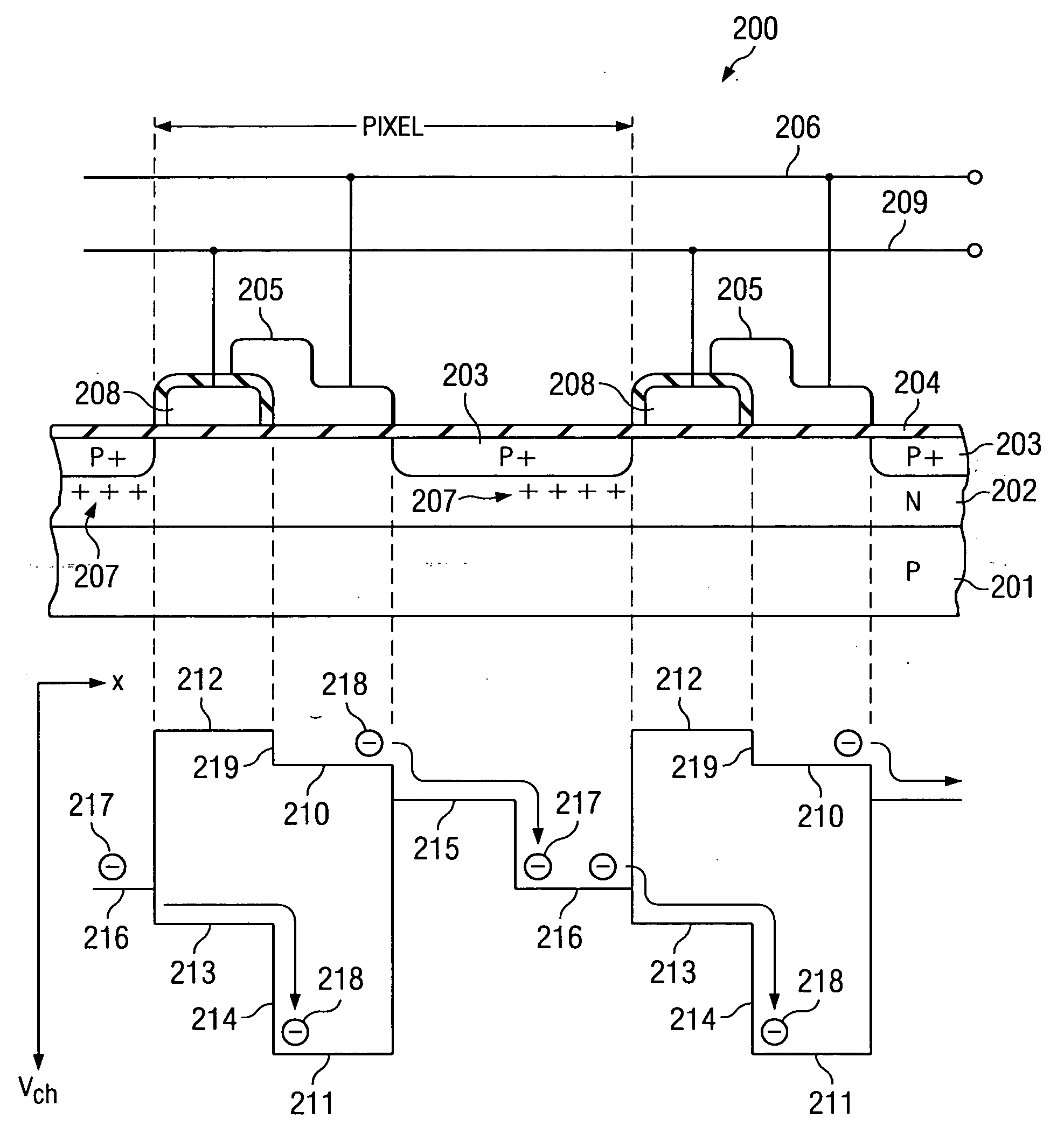
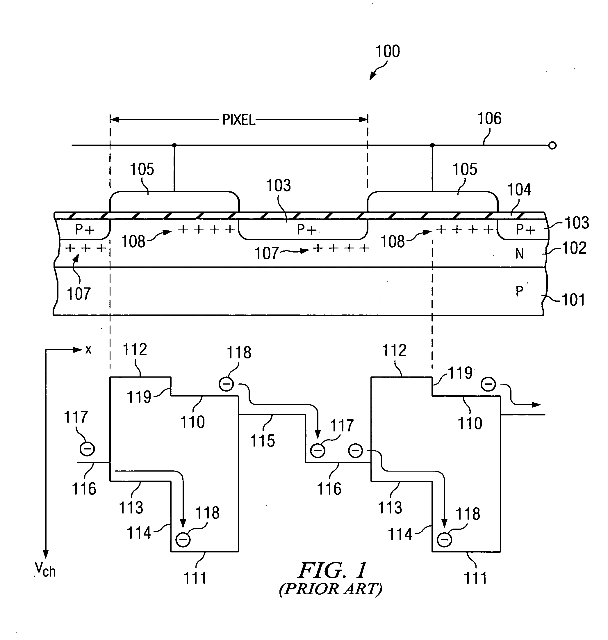
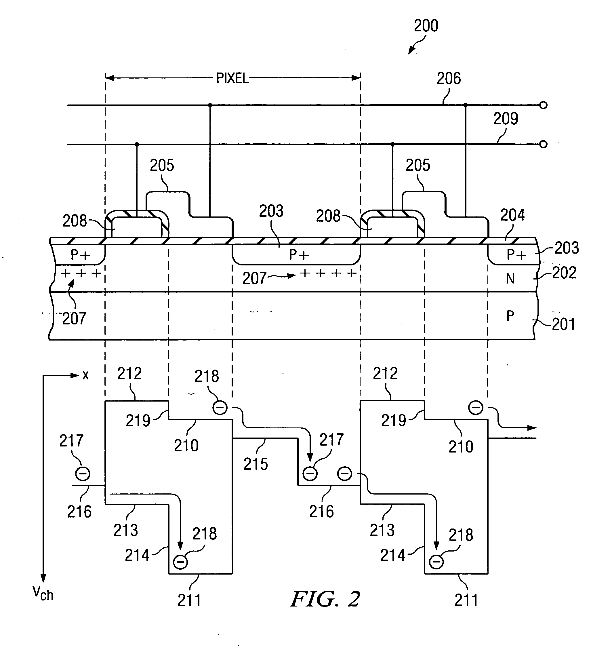
[0012] In FIG. 1 the drawing 100 represents simplified cross section through the middle of the CCD channel of a standard prior art VP CCD device together with corresponding channel potential profiles in various device sections for the high and low gate biasing levels. P-type substrate 101 has n-type buried channel implant 102 near its surface. Oxide layer 104 separates the substrate from poly silicon gate electrodes 105 that are connected together and to a bias terminal by metal wiring 106. P+ type Virtual Phase implant 103 has been implanted between gate electrodes 105. The directionality of charge transfer is created by placing additional implants 107 and 108 near the surface of the substrate just under poly gate electrodes 105 and VP gate region 103. The resulting structure, after depletion of excess mobile charge, creates potential profile in each pixel described by segments 116, 112, 119, 110, 115, and 116, for low gate biasing level and by segments 116, 113, 114, 111, 115, and...


PUM


Abstract

The charge coupled device includes a clocked barrier pixel architecture that has a two phase gate structure that substantially reduces clock-induced dark current.

Description

FIELD OF THE INVENTION [0001] The present invention relates to solid-state image sensors and specifically to a class of Virtual Phase (VP) charge coupled device (CCD) image sensors that have high sensitivity, high blue response, low smear, and that multiply collected charge using single carrier impact ionization process before charge conversion into a voltage. BACKGROUND OF THE INVENTION [0002] A typical image sensor senses light by converting impinging photons into electrons that are integrated (collected) in the image sensing area array of pixels. After completion of integration collected electrons are transported into a suitable storage area by the CCD transfer process and further from the storage area into the detection node where electron charge is converted into a voltage. The resulting voltage is then supplied to the output terminals of the sensor. In Full Frame (FF) and Frame Transfer (FT) devices charge is integrated directly in the column pixels of the image area array reg...

Claims


Application Information

Patent Timeline
Patent Type & Authority Applications(United States)
IPC IPC(8): H01L27/148H01L29/768H04N5/359H04N5/361H04N5/3725
CPCH01L27/14806H01L27/1485H01L27/14887
Inventor HYNECEK, JAROSLAV
Owner TEXAS INSTR INC
Why Eureka
Try Eureka