Semiconductor storage device and method of manufacturing the same

a technology of semiconductor storage devices and semiconductors, applied in the field of semiconductor storage devices, can solve problems such as loss of trapped charges, and achieve the effect of restoring crystal defects and enhancing memory characteristics

Inactive Publication Date: 2005-02-10
SEIKO EPSON CORP
View PDF2 Cites 12 Cited by
  • Summary
  • Abstract
  • Description
  • Claims
  • Application Information

AI Technical Summary

Benefits of technology

[0006] In the above semiconductor storage device, the thermal oxide film 132 serves to recover damage due to etching when patterning the gate electrode, and restore crystal defect. This thermal oxide film 132, however, is not formed on a side surface of the ONO film 120. Specifi

Problems solved by technology

This contributes to loss of trapped charges such that

Method used


Image

  • Semiconductor storage device and method of manufacturing the same
  • Semiconductor storage device and method of manufacturing the same
  • Semiconductor storage device and method of manufacturing the same

Examples


first exemplary embodiment

[0035] 1.1 First Exemplary Embodiment

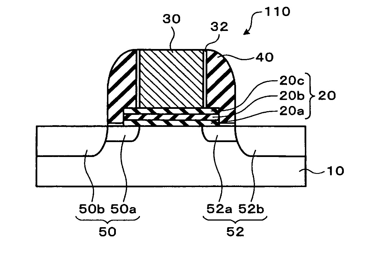
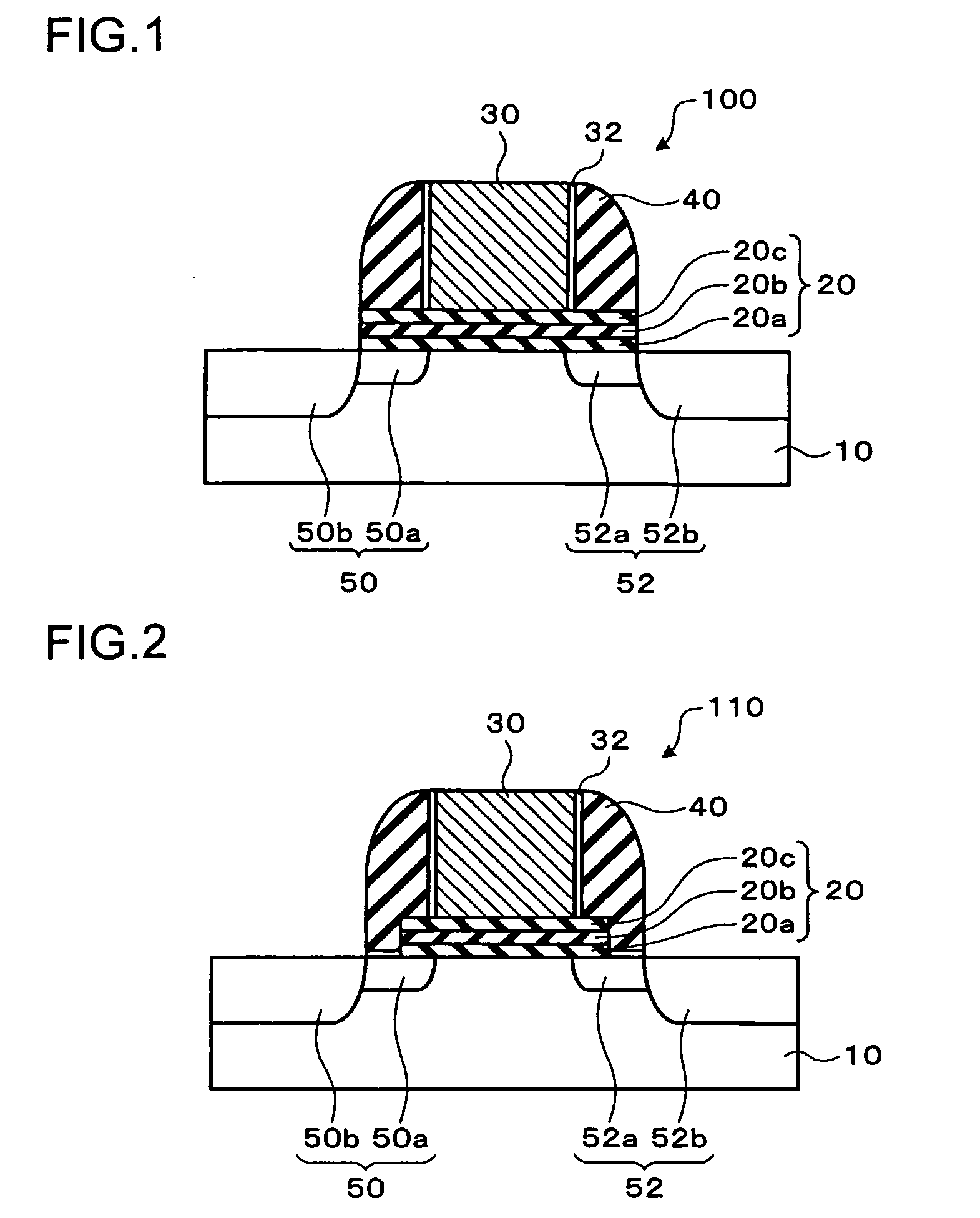
[0036]FIG. 1 is a schematic showing a semiconductor storage device according to a first exemplary embodiment. In a semiconductor storage device 100, a stacked body 20 including a first insulating layer 20a, a charge trapping layer 20b, and a second insulating layer 20c is formed above a semiconductor substrate 10, which is a semiconductor layer. A gate electrode 30 is formed above the stacked body 20. A side wall insulating layer 40 is formed over a side surface of the gate electrode 30 with a protective film 32 therebetween. The end surface of the stacked body 20 is positioned outside the end surface of the gate electrode 30. In the present exemplary embodiment, the case where the end surface of the stacked body 20 is flush with the end surface of the side wall insulating layer 40 is exemplified. In the semiconductor substrate 10, a source region 50 and a drain region 52 having an LDD structure are provided.

second exemplary embodiment

[0037] 1.2 Second Exemplary Embodiment

[0038] A semiconductor storage device 110 according to a second exemplary embodiment will be described referring to FIG. 2. The semiconductor storage device 10 according to the second exemplary embodiment is an example where the width of the stacked body 20 is different from that of the semiconductor storage device 100 according to the first exemplary embodiment. For the same members, the same numerals are given, and detailed description will be omitted.

[0039] In the semiconductor storage device 10 shown in FIG. 2, the end surface of the stacked body 20 is positioned outside the end surface of the gate electrode 30. The width of the stacked body 20 is smaller than the width of the under surface of the side wall insulating layer 40. The distance between the end surface of the stacked body 20 and the end surface of the gate electrode 30 may be 10 nanometers or more. When the distance between the end surface of the stacked body 20 and the end surf...


PUM


Abstract

A semiconductor storage device showing a good memory characteristic, and a manufacturing method thereof, includes a semiconductor layer, a stacked body including a first insulating layer, a charge trapping layer, and a second insulating layer that are provided above the semiconductor layer, a gate electrode provided above the stacked body, a side wall insulating layer provided at the side of the gate electrode, and impurity regions and provided in the semiconductor layer. The end surface of the stacked body is positioned outside the end surface of the gate electrode.

Description

BACKGROUND OF THE INVENTION [0001] 1. Field of Invention [0002] The present invention relates to an insulating-film trapping type non-volatile semiconductor storage device (hereinafter “MONOS”) and a manufacturing method thereof. [0003] 2. Description of Related Art [0004] As a semiconductor storage device capable of electrically writing and erasing, there has been a non-volatile semiconductor storage device, which can retain stored date even when power for a memory is eliminated. As such a semiconductor storage device, there is a MONOS type semiconductor storage device. [0005] A MONOS type semiconductor storage device 1000 according to a related art example is shown in FIG. 9. In the semiconductor storage device 1000, a gate electrode 130 is formed above a semiconductor substrate 110 with an ONO film 120 therebetween. A thermal oxide film 132 is formed on a side surface of the gate electrode 130, and a surface of the semiconductor substrate 110 where a side wall insulating layer 14...

Claims


Application Information

Patent Timeline
IPC IPC(8): H01L21/28H01L21/8247H01L21/336H01L27/10H01L27/115H01L29/788H01L29/792
CPCH01L21/28282H01L29/792H01L29/66833H01L29/40117
Inventor MORI, KATSUMI
Owner SEIKO EPSON CORP
Why Eureka
Try Eureka