
Semiconductor package including flip chip

Inactive Publication Date: 2005-02-10
AMKOR TECH SINGAPORE HLDG PTE LTD
View PDF99 Cites 8 Cited by
  • Summary
  • Abstract
  • Description
  • Claims
  • Application Information

AI Technical Summary

Benefits of technology

[0010] The structural attributes of the present semiconductor package impart thereto the ability to withstand severe environments for prolonged durations of time. In this regard, the structure of the present semiconductor package provides substantial moisture resistance characteristics. In addition, the input / output terminals defined by the exposed first surfaces of the leads can be mounted directly to an external device such as a motherboard, thereby minimizing the thickness of the semiconductor package / motherboard assembly. The configuration of the lead frame used in the manufacture of the present semiconductor package further minimizes the cost associated with the fabrication thereof.

Problems solved by technology

However, currently known semiconductor packages fabricated using the flip chip bonding method described above possess certain deficiencies which detract from their overall utility.
More particularly, since such semiconductor package employs a printed circuit board component which is costly, the manufacturing cost of the entire semiconductor package is itself significantly increased.
In this regard, the cost of the printed circuit board component is extremely high due to the complexity of its manufacturing process, with the printed circuit board component accounting for more than sixty percent of the total cost of the semiconductor package employing the same.
As indicated above, this high cost of the printed circuit board component results in an increased cost in the semiconductor package.
Another drawback associated with the printed circuit board component is that the same typically includes a resin layer and a solder mask which each have high water absorptivity.
The susceptibility of the resin layer and solder mask to high levels of water absorption causes the semiconductor package to have a low level of resistance to moisture.
As a result, the life span of the semiconductor package is drastically shortened when the same is used in regions of high humidity.
A further problem pertains to the conductive balls which are fused to the bottom surface of the printed circuit board component of the semiconductor package.
In this regard, the conductive balls are typically thicker than the semiconductor package itself, thus resulting in a significant increase in the overall thickness of the semiconductor package assembly including the conductive balls.

Method used


Image

  • Semiconductor package including flip chip
  • Semiconductor package including flip chip
  • Semiconductor package including flip chip

Examples


Embodiment Construction

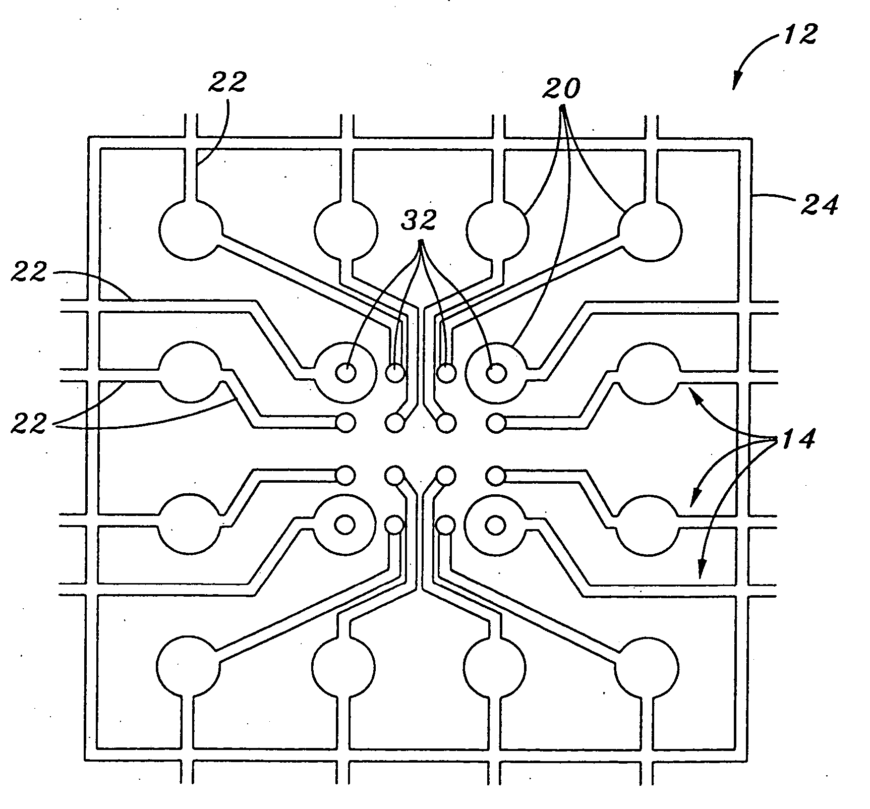
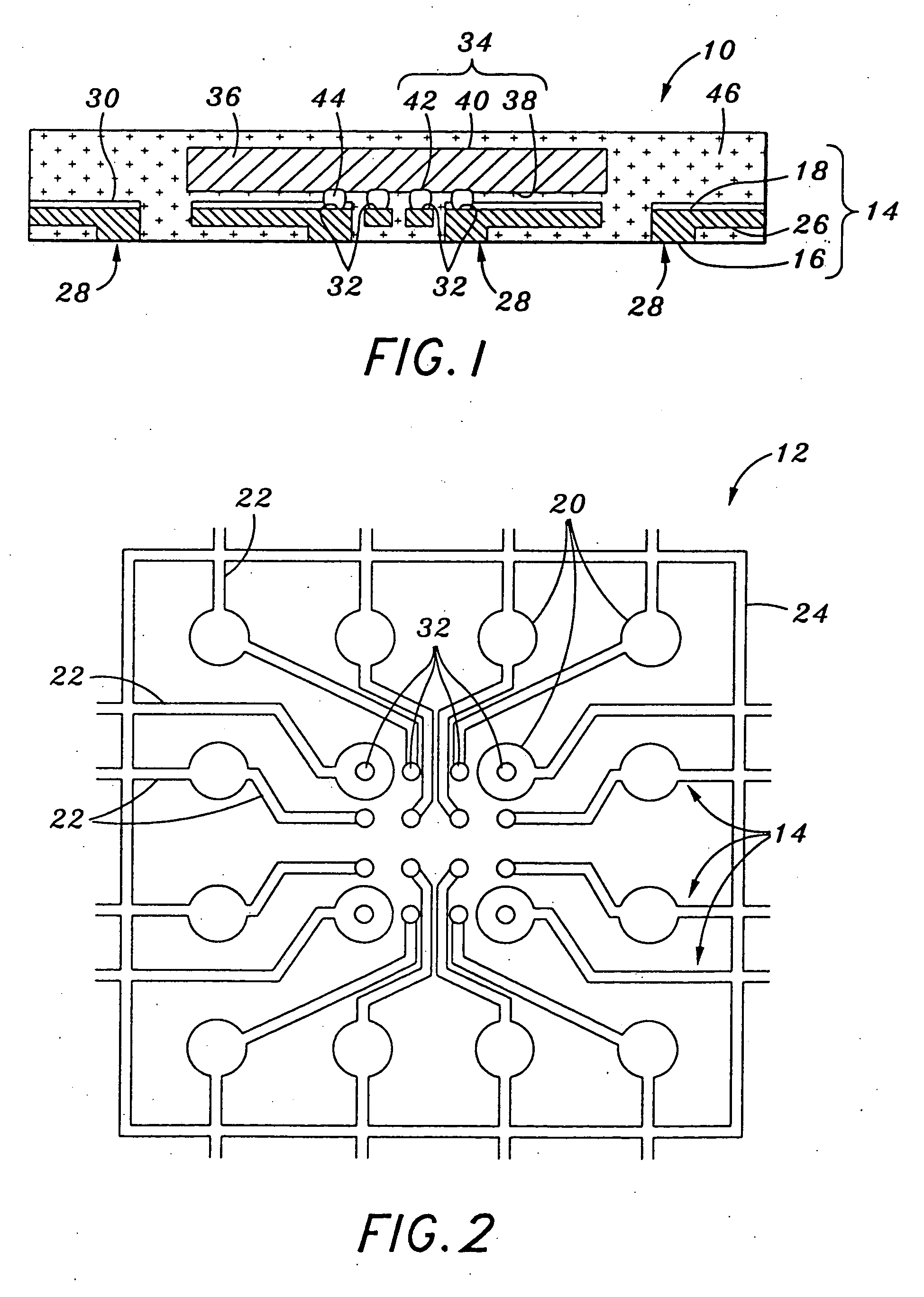
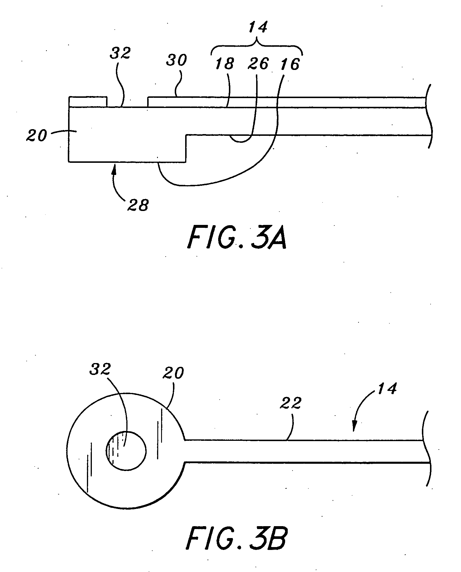
[0018] Referring now to the drawings wherein the showings are for purposes of illustrating a preferred embodiment of the present invention only, and not for purposes of limiting the same, FIG. 1 illustrates in cross section a semiconductor package 10 constructed in accordance with the present invention. The semiconductor package 10 includes a lead frame 12 which is shown in FIG. 2. The lead frame 12 includes a plurality of leads 14, each of which defines a generally planar first (bottom) surface 16 and an opposed, generally planar second (top) surface 18. Each of the leads 14 further defines a circularly configured pad portion 20 and at least one elongate connecting bar portion 22 integrally connected to and extending from the pad portion 20. The leads 14 are arranged within the lead frame 12 such that the pad portions 20 are segregated into an outer set of twelve pad portions 20 which are arranged in a generally square pattern and an inner set of four pad portions 20 which are loca...


PUM


Abstract

A semiconductor package comprising a plurality of leads. Each of the leads defines opposed first and second surfaces. Also included in the semiconductor package is a semiconductor chip which defines opposed first and second surfaces, and includes a plurality of input / output pads disposed on the first surface thereof. A plurality of conductive bumps are used to electrically connect the input / output pads of the semiconductor package to the second surfaces of respective ones of the leads. An encapsulant portion of the semiconductor package covers the semiconductor chip, the conductive bumps, and the second surfaces of the leads such that at least portions of the first surfaces of the leads are exposed within the encapsulant portion.

Description

CROSS-REFERENCE TO RELATED APPLICATIONS [0001] The present application claims priority to Korean Patent Application No. 2000-86246 entitled SEMICONDUCTOR PACKAGE filed Dec. 29, 2000. STATEMENT RE: FEDERALLY SPONSORED RESEARCH / DEVELOPMENT [0002] (Not Applicable) BACKGROUND OF THE INVENTION [0003] 1. Field of the Invention [0004] The present invention relates generally to semiconductor packages, and more particularly to a semiconductor package which includes a flip chip and is specifically configured to provide a thinner profile and superior moisture resistance capabilities as compared to flip chip semiconductor packages known in the prior art. [0005] 2. Description of the Related Art [0006] The recent trend in the electronics industry has been toward the fabrication of lighter, thinner, more simplistic and miniaturized semiconductor packages. To achieve these objectives, there has been developed semiconductor packages fabricated through the use of a flip chip bonding method wherein a...

Claims


Application Information

Patent Timeline
IPC IPC(8): H01L23/31H01L23/495H01L23/12
CPCH01L23/3107H01L23/4951H01L2224/16245H01L2224/16H01L2924/01079H01L23/49551H01L2224/05571H01L2224/05573H01L2924/00014H01L2224/06131H01L2224/05599H01L23/12
Inventor PAEK, JONG SIK
Owner AMKOR TECH SINGAPORE HLDG PTE LTD
Learn More