Semiconductor device and method for manufacturing the same

a technology of semiconductor devices and semiconductor films, applied in the field of semiconductor devices, can solve the problem of lowering the effective dielectric constant of the insulating film as a whol

Active Publication Date: 2005-02-10
EBARA CORP
View PDF9 Cites 35 Cited by
  • Summary
  • Abstract
  • Description
  • Claims
  • Application Information

AI Technical Summary

Benefits of technology

[0014] The present invention has been made in view of the above situation in the related art. It is therefore an object of the present invention to provide a semiconductor device which has a highly reliable multi-level interconnect structure having a low effective dielectric constant and which can be easily manufactured with a relatively inexpensive process, and a method for manufacturing the semiconductor device.

Problems solved by technology

This can lower the effective dielectric constant of the insulating film as a whole.

Method used


Image

  • Semiconductor device and method for manufacturing the same
  • Semiconductor device and method for manufacturing the same
  • Semiconductor device and method for manufacturing the same

Examples


experimental example

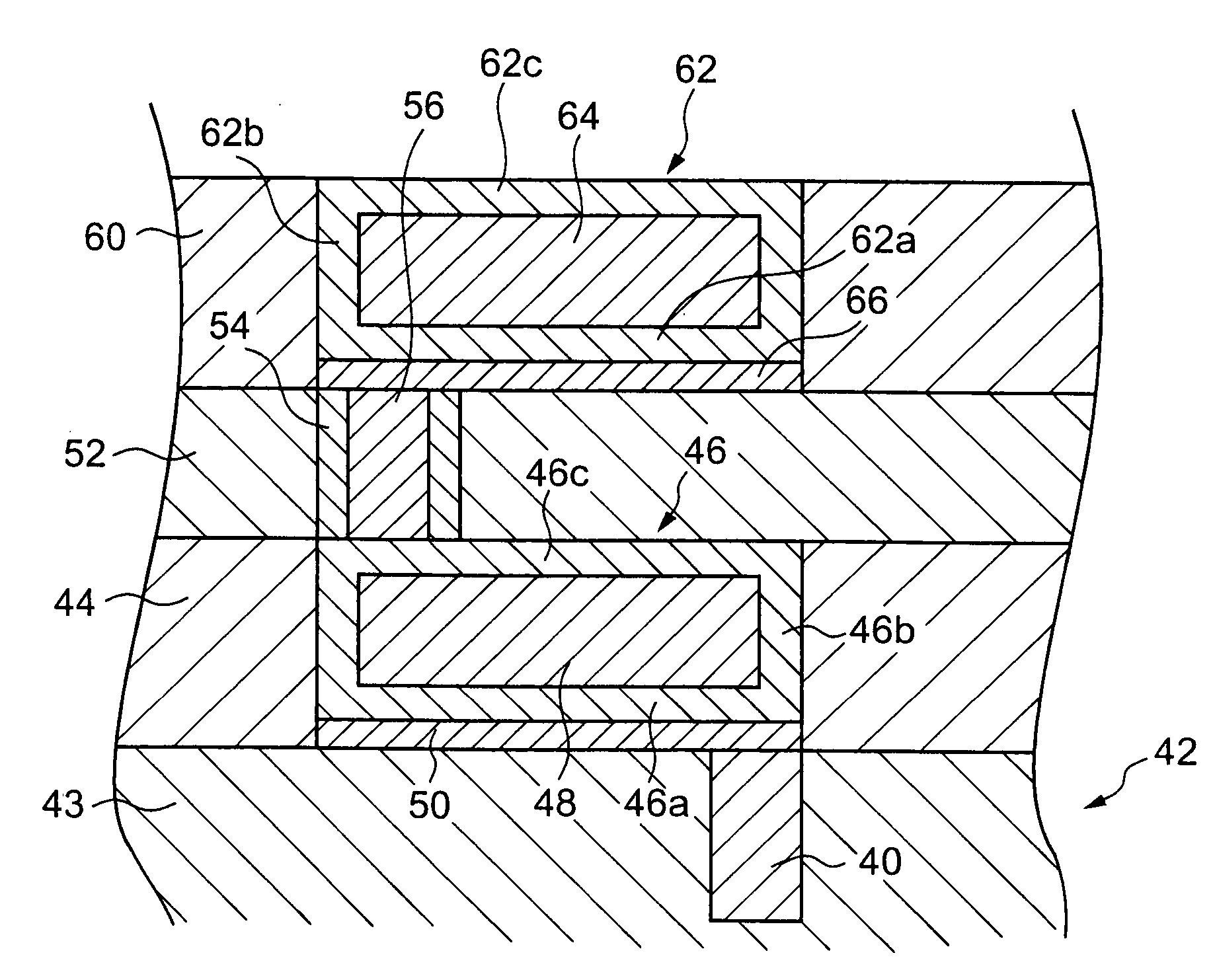
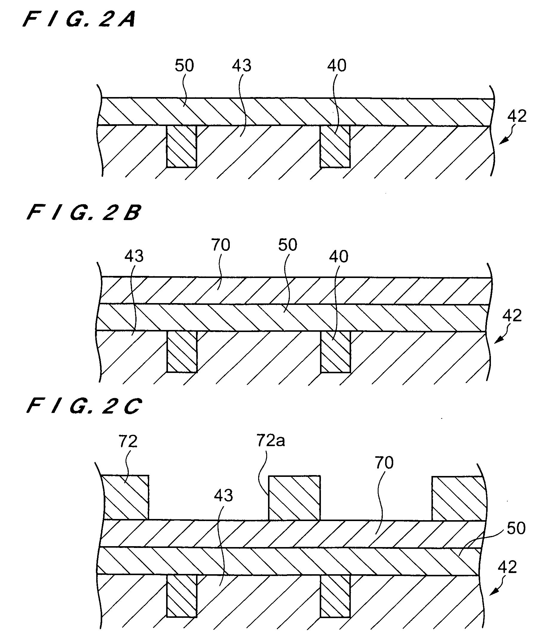
[0079] A description will now be given of an experimental example in which a semiconductor device having a multi-level interconnect structure as shown in FIG. 1 was actually manufactured by the process shown in FIGS. 2 to 10.

[0080] First, a 5 nm-thick liner layer 50 of Co was formed by sputtering on the surface of the insulating film 43, after CMP, of the semiconductor substrate 42 having plugs 40 shown in FIG. 2A. Thereafter, as shown in FIG. 2B, a 20 nm-thick barrier layer 70 of a COWB alloy was formed on the liner layer (Co layer) 50 by electroless plating utilizing the liner layer 50 as a catalyst.

[0081] Next, as shown in FIG. 2C, openings (trenches) 72a e.g. having a width of 50 nm, a depth of 100 nm and an AR (aspect ratio) of 2.0 were formed by photoresist patterning with a resist 72. Thereafter, as shown in FIG. 3A, copper as an interconnect material was embedded selectively in the trenches 72a in a bottom-up manner by electroless plating utilizing the barrier layer (CoWB ...


PUM

PropertyMeasurementUnit
dielectric constantaaaaaaaaaa
thicknessaaaaaaaaaa
depthaaaaaaaaaa

Abstract

A semiconductor device including a highly reliable multi-level interconnect structure having a low effective dielectric constant and which can be easily manufactured with a relatively inexpensive process, and a method for manufacturing the semiconductor device. The semiconductor device includes a lower-level interconnect and an upper-level interconnect, each surrounded by a barrier layer, and a via plug surrounded by a barrier layer and electrically connecting the lower-level interconnect and the upper-level interconnect.

Description

BACKGROUND OF THE INVENTION [0001] 1. Field of the Invention [0002] The present invention relates to a semiconductor device and a method for manufacturing the same, and more particularly to a semiconductor device having a multi-level interconnect structure in which lower-level interconnects (first-level interconnects) and upper-level interconnects (second-level interconnects) are electrically connected by via plugs embedded in via holes, and a method for manufacturing the semiconductor device. [0003] 2. Description of the Related Art [0004] A process which comprises embedding a metal (electrical conductor) in interconnect trenches and via holes (so-called dual damascene process) is coming into practical use as a process for forming multi-level interconnects in the manufacturing of a semiconductor device. According to this process, aluminum, or more recently a metal such as copper, silver, or the like, is embedded in interconnect trenches and via holes which have previously been form...

Claims


Application Information

Patent Timeline
Patent Type & Authority Applications(United States)
IPC IPC(8): C25D7/12H01L21/288C23C18/16H01L21/768H01L23/522H01L23/532
CPCH01L21/76852H01L21/76885H01L23/53252H01L23/53238H01L23/5226H01L2924/0002H01L2924/00
Inventor INOUE, HIROAKISUSAKI, AKIRA
Owner EBARA CORP
Why Eureka
Try Eureka