Per column one-bit ADC for image sensors

Active Publication Date: 2005-02-24
MICRON TECH INC
View PDF27 Cites 79 Cited by
  • Summary
  • Abstract
  • Description
  • Claims
  • Application Information

AI Technical Summary

Benefits of technology

The present invention provides an improved analog-to-digital converter for image sensors, which reduces the circuitry and power consumption of the image sensor.
The above and other features and advantages are achieved in various embodiments of the invention by providing a per column one-bit analog-to-digital converter for an image sensor. The analog-to-digital converter utilizes the difference between a reference signal current and a pixel signal current to obtain

Problems solved by technology

Unfortunately, variation in the power supply, noise and precision of the reference voltage adve

Method used


Image

  • Per column one-bit ADC for image sensors
  • Per column one-bit ADC for image sensors
  • Per column one-bit ADC for image sensors

Examples


Example

In the following detailed description, reference is made to the accompanying drawings, which are a part of the specification, and in which is shown by way of illustration various embodiments whereby the invention may be practiced. These embodiments are described in sufficient detail to enable those skilled in the art to make and use the invention. It is to be understood that other embodiments may be utilized, and that structural, logical, and electrical changes, as well as changes in the materials used, may be made without departing from the spirit and scope of the present invention.

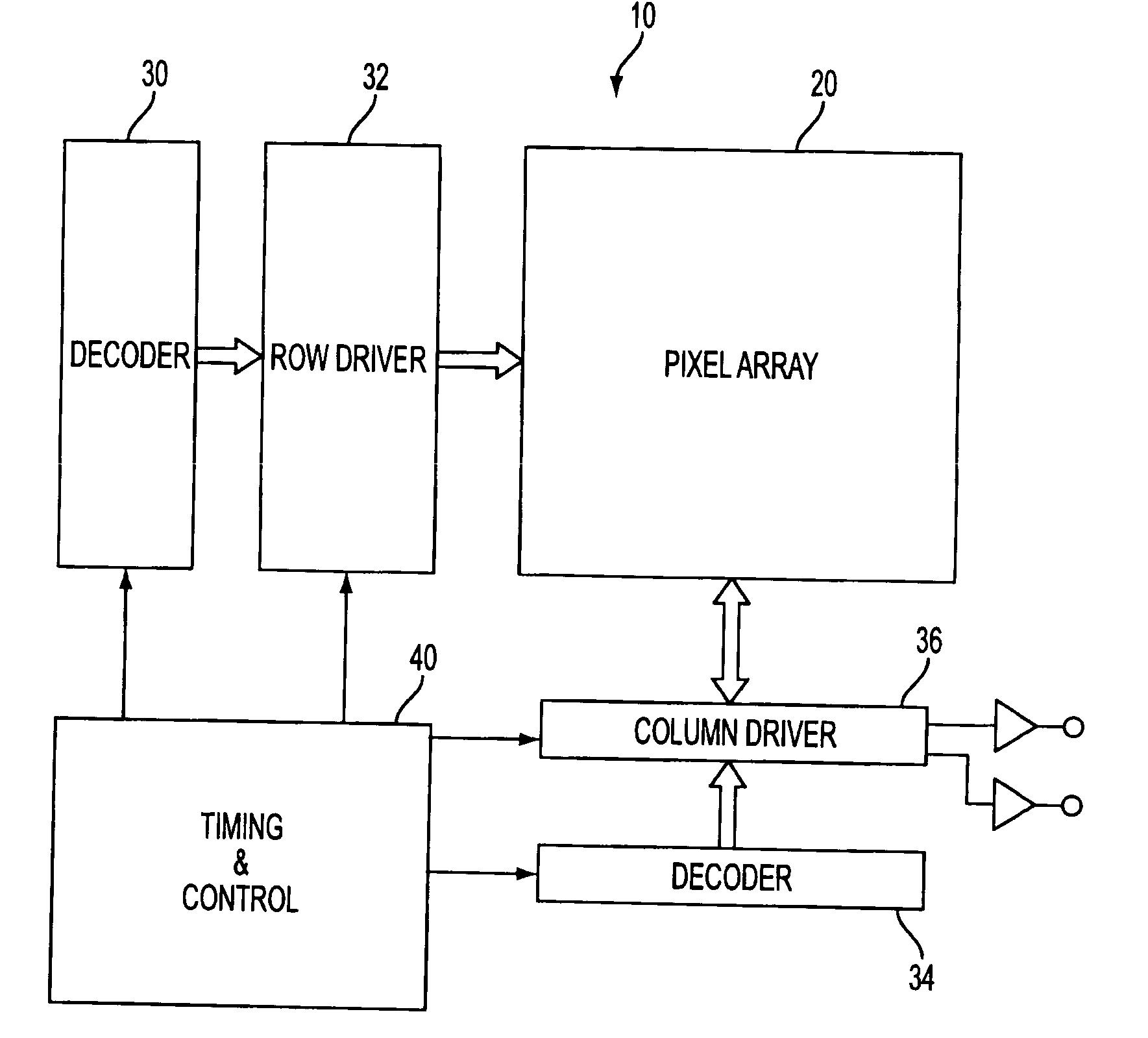
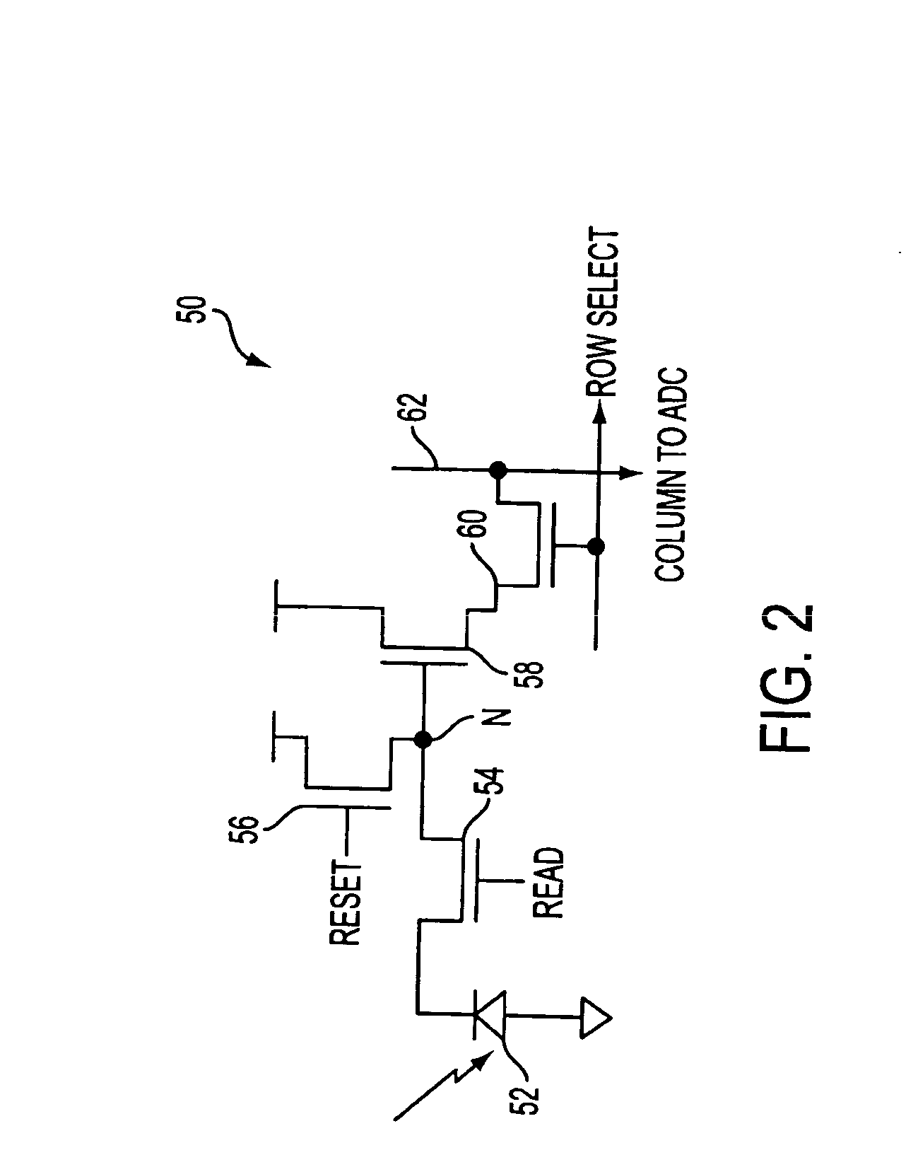
Now referring to the figures, where like reference numbers designate like elements, FIG. 2 shows an exemplary pixel circuit 50 used in a CMOS imager such as the imager 10 illustrated in FIG. 1. The pixel 50 includes a photosensor 52 (e.g., photodiode, photogate, etc.), floating diffusion node N, transfer transistor 54, reset transistor 56, source follower transistor 58 and row select transistor 60. Th...


PUM


Abstract

A per column one-bit analog-to-digital converter for an image sensor. The analog-to-digital converter utilizes the difference between a reference signal current and a pixel signal current to obtain a digital output representative of the analog pixel signal in an efficient and simple manner. The output of the one-bit analog-to-digital converter is fed to a counter to give a representation of the brightness of the light-to-charge conversion in the associated pixel. The analog-to-digital converter does not use a reference voltage and precision elements and thus, does not suffer from power supply, noise and precision variations.

Description

FIELD OF THE INVENTION The invention relates generally to imaging devices, and more particularly to a per column one-bit analog-to-digital converter (ADC) for an image sensor. BACKGROUND Imaging devices, including charge coupled devices (CCD) and complementary metal oxide semiconductor (CMOS) imagers, are commonly used in photo-imaging applications. A CMOS imager circuit includes a focal plane array of pixel cells, each one of the cells including either a photogate, photoconductor or a photodiode overlying a substrate for accumulating photo-generated charge in the underlying portion of the substrate. A readout circuit is connected to each pixel cell and includes at least an output field effect transistor formed in the substrate and a charge transfer section formed on the substrate adjacent the photogate, photoconductor or photodiode having a sensing node, typically a floating diffusion node, connected to the gate of an output transistor. The imager may include at least one electr...

Claims


Application Information

Patent Timeline
IPC IPC(8): H04N5/357H04N5/378
CPCH04N5/335H04N25/00
Inventor BAKER, R. JACOB
Owner MICRON TECH INC
Why Eureka
Try Eureka