Pattern forming method, wiring pattern forming method, electro-optical device, and electronic apparatus

a technology of pattern forming and wire forming, applied in the field of pattern forming method, wiring pattern forming method, electrooptical device, electronic apparatus, can solve the problems of requiring an expensive and large device, and achieve the effect of simple and inexpensive devi

Active Publication Date: 2005-02-24
INTELLECTUAL KEYSTONE TECH LLC
View PDF5 Cites 31 Cited by
  • Summary
  • Abstract
  • Description
  • Claims
  • Application Information

AI Technical Summary

Benefits of technology

[0006] An aspect of the invention can provide a pattern forming method capable of patterning a thin film by a simplified and inexpensive device. In addition, it is another object of th

Problems solved by technology

According to the technology disclosed above, ultraviolet (UV) rays or an electronic beam is radiated onto the substrate t

Method used


Image

  • Pattern forming method, wiring pattern forming method, electro-optical device, and electronic apparatus
  • Pattern forming method, wiring pattern forming method, electro-optical device, and electronic apparatus
  • Pattern forming method, wiring pattern forming method, electro-optical device, and electronic apparatus

Examples


Embodiment Construction

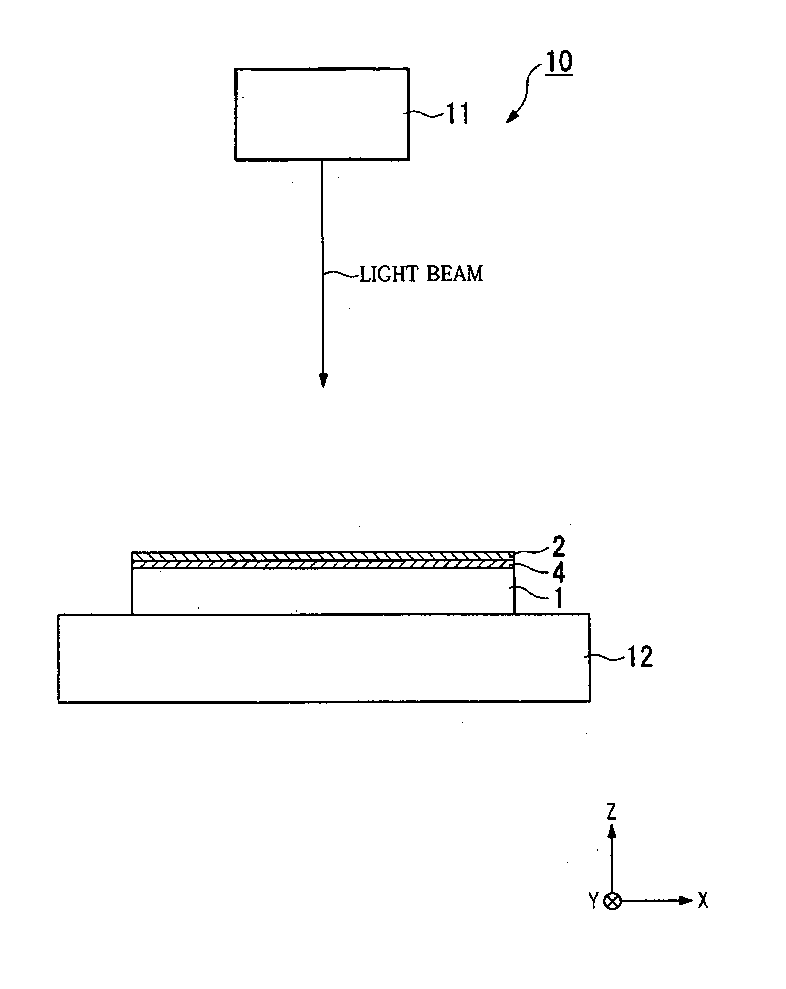
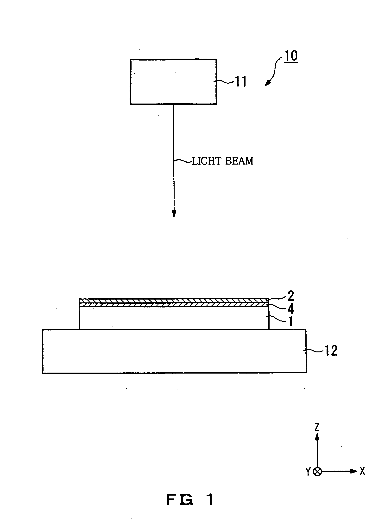
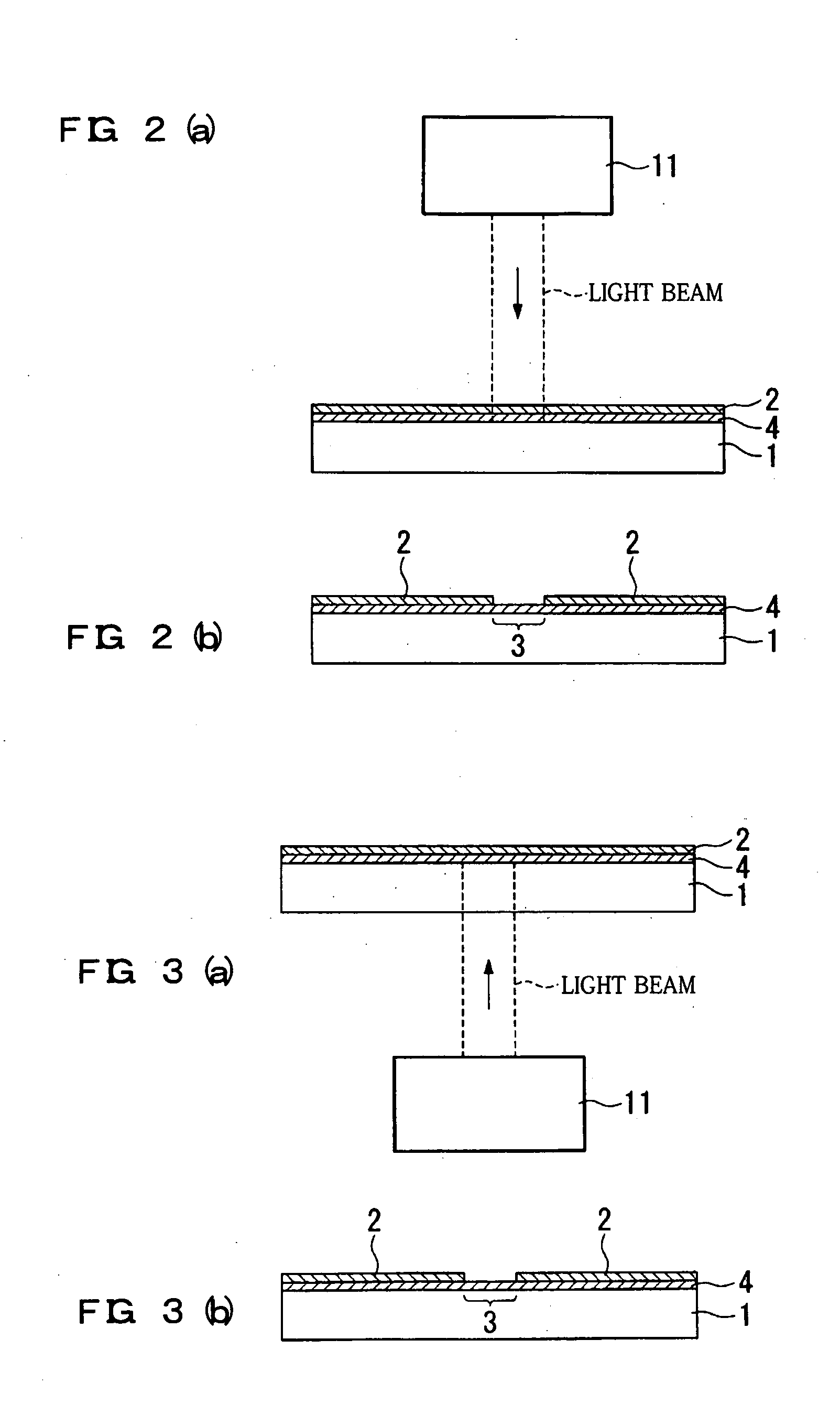
[0034] Hereinafter, a pattern forming method according to the invention will be described with reference to the accompanying drawings. FIG. 1 is a schematic diagram illustrating an exemplary embodiment of a pattern forming apparatus used in the thin film pattern forming method according to the invention. In FIG. 1, the pattern forming apparatus 10 can include a laser source 11 for radiating a laser beam having a predetermined wavelength and a stage 12 for supporting a base member 1 which is a processing target. A photothermal conversion layer 4 is provided on the surface of the base member 1 and a thin film 2 is provided on the photothermal conversion layer 4. In this exemplary embodiment, a near-infrared semiconductor laser (with a wavelength of 830 nm) is used as the laser source 11.

[0035] In the following description, it is assumed that a predetermined direction in a horizontal plane is an X axis direction, a direction perpendicular to the X axis direction in the horizontal plan...


PUM

PropertyMeasurementUnit
Energyaaaaaaaaaa

Abstract

Aspects of the invention can provide a patterning forming method capable of patterning a thin film by a simple and inexpensive device. The thin film can be provided on a base member including a photothermal conversion material that converts optical energy into thermal energy and light is radiated onto the base member to remove the thin film corresponding to a light-radiated region, such that the thin film is patterned.

Description

BACKGROUND OF THE INVENTION [0001] 1. Field of Invention [0002] Aspects of the invention relate to a pattern forming method of forming a thin film pattern on a base member, a wiring pattern forming method using the thin film pattern, an electro-optical device, and an electronic apparatus. [0003] 2. Description of Related Art [0004] Related methods of manufacturing devices having minute wiring patterns, such as semiconductor integrated circuits, the photolithography method has been widely used, and device manufacturing methods using a liquid droplet ejecting method (an inkjet method) have also been of interest. When the minute wiring patterns are formed using the liquid droplet ejecting method, a method of patterning a lyophobic region and a lyophilic region on a base member in advance so as to enhance precision of the pattern line width and selectively arranging droplets on the lyophilic region has been suggested. Further, for example in Japanese Unexamined Patent Application Public...

Claims


Application Information

Patent Timeline
IPC IPC(8): B05D3/12G03F7/004B05D7/00B32B3/00G02F1/1343G03F7/11G03F7/36H01L21/027H01L51/50H05B33/10H05B33/14H05B33/26H05K3/06H05K3/10H05K3/12H05K3/14
CPCB82Y30/00H05K3/1208H05K3/125Y10T428/24917H05K2203/107H05K2203/1173Y10S430/146H05K2201/0112G03F7/2018G03F7/202
Inventor TOYODA, NAOYUKI
Owner INTELLECTUAL KEYSTONE TECH LLC
Why Eureka
Try Eureka