Bipolar/thin film SOI CMOS structure and method of making same

a thin film, bipolar silicon germanium bipolar transistor technology, applied in the field of wafer scale technology, can solve the problems of slowed circuitry, objectionable loss of silicon germanium bipolar heterojunction transistor/cmos circuitry, and inability to isolate rf signals fully

Inactive Publication Date: 2005-03-03
NORTHROP GRUMAN CORP
View PDF6 Cites 9 Cited by
  • Summary
  • Abstract
  • Description
  • Claims
  • Application Information

AI Technical Summary

Problems solved by technology

When used in microwave applications, present day silicon germanium bipolar heterojunction transistor / CMOS circuitry tends to be objectionably lossy due to low resistivity silicon material in which the transistors are fabricated.
Further, the circuitry is slowed down and cannot fully isolate the RF signals when operating in a switching mode due to p-n junction capacitance.

Method used


Image

  • Bipolar/thin film SOI CMOS structure and method of making same
  • Bipolar/thin film SOI CMOS structure and method of making same
  • Bipolar/thin film SOI CMOS structure and method of making same

Examples


Embodiment Construction

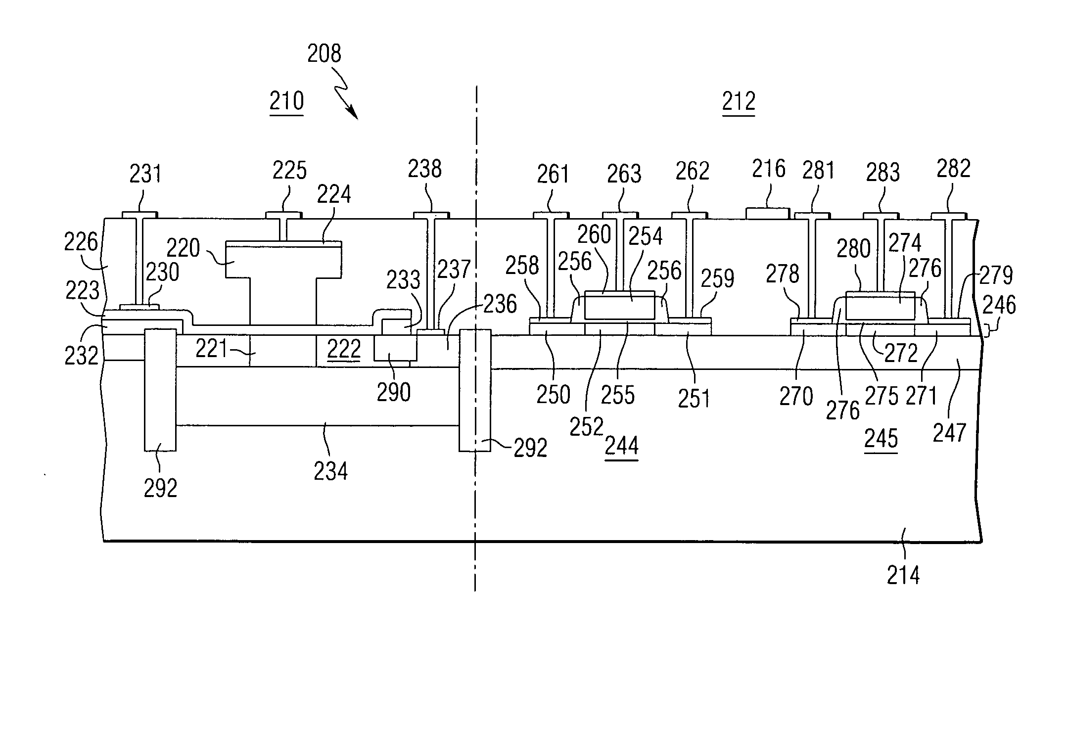
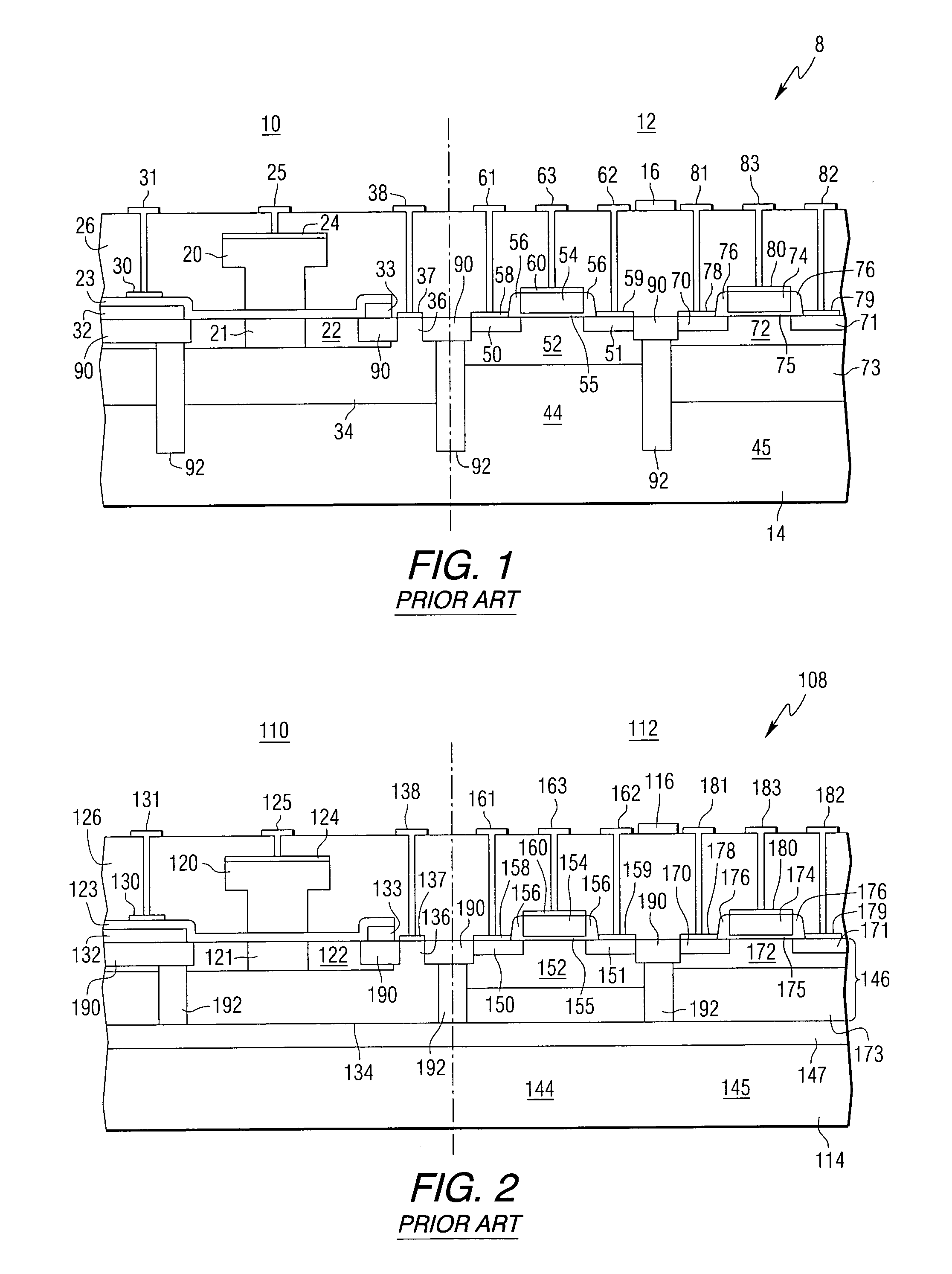
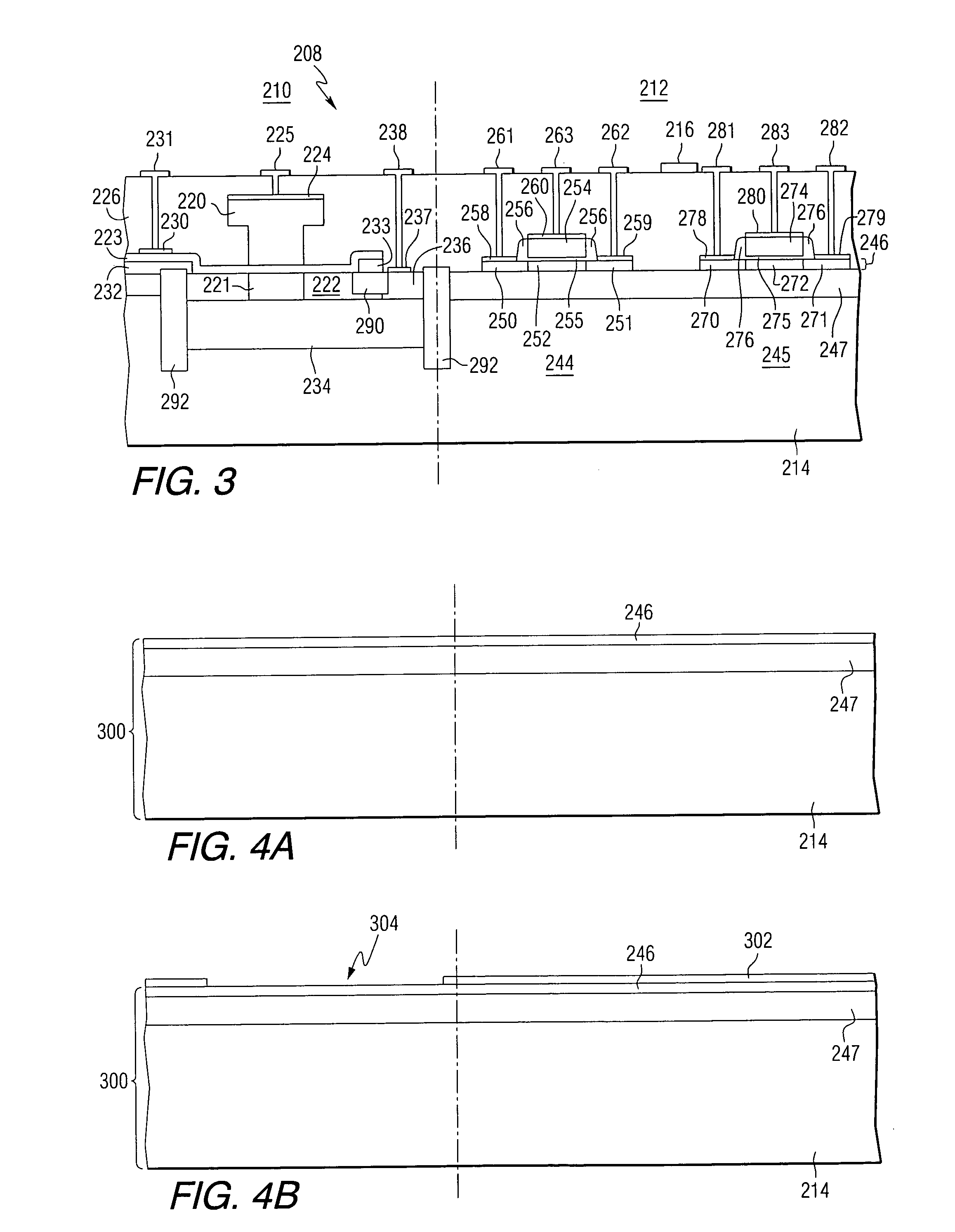
[0015]FIG. 1 illustrates a prior art silicon-based wafer structure arrangement 8 wherein a silicon germanium bipolar heterojunction transistor 10 and a CMOS transistor device 12 are formed on the same silicon wafer substrate 14. For convenience, in the Figures, the bipolar transistor and CMOS device are shown adjacent one another. In actuality the wafer arrangement may contain a multitude of such elements, and not necessarily adjacent, along with other circuit components, including signal transmission lines, one of which, 16, is illustrated.

[0016] The bipolar transistor 10 includes an emitter 20, a collector 21 formed in epitaxially grown collector layer 22, and a base 23 interposed between the emitter and collector. The emitter 20 and collector 21 are of one conductivity type for example, n-type, while the base 23 is of an opposite conductivity p-type. For superior operation, and high speed performance, the base 23 is of a silicon germanium composition, generally 90% silicon and 1...


PUM


Abstract

A semiconductor wafer structure which includes at least one bipolar transistor defined in the semiconductor wafer structure as well as at least one CMOS transistor device also defined in the semiconductor wafer structure. The CMOS transistor device is comprised of a thin film of semiconductor on an insulating layer with each transistor of the CMOS transistor device being defined in the thin film. The bipolar transistor has a plurality of semiconductor layers of predetermined conductivities, without any of the semiconductor layers of the bipolar transistor extending into the area occupied by the CMOS transistor device. A method of fabricating the structure is also disclosed.

Description

BACKGROUND OF THE INVENTION [0001] 1. Field of the Invention [0002] The invention in general relates to wafer scale technology and more particularly to an improved silicon germanium bipolar transistor / CMOS structure. [0003] 2. Description of Related Art [0004] Silicon germanium bipolar heterojunction transistors have been developed and compared to conventional silicon bipolar transistors are faster, more energy efficient and are cost competitive, if not cheaper than the silicon variety. [0005] These silicon germanium bipolar heterojunction transistors are used not only in such applications as ASICs (application specific integrated circuits) but are used in other fields including communications systems and military radars. These devices provide much improved performance at high frequencies and at reduced temperatures and reduced power consumption. [0006] The silicon germanium bipolar heterojunction transistors maintain compatibility with CMOS (complementary metal-oxide semiconductor)...

Claims


Application Information

Patent Timeline
Patent Type & Authority Applications(United States)
IPC IPC(8): H01L21/8249H01L21/84H01L27/06H01L27/12
CPCH01L21/8249H01L27/1203H01L27/0623H01L21/84
Inventor TURLEY, ALFRED P.
Owner NORTHROP GRUMAN CORP
Why Eureka
Try Eureka