Method of manufacturing ultrasound transducer device having acoustic backing

a manufacturing method and ultrasound technology, applied in piezoelectric/electrostrictive transducers, electrostatic transducers, magnets, etc., can solve the problems of reducing the quality of the acoustic image obtained from reflection within the patient, requiring ceramic manufacturing processes, and acoustic energy transmitted in the direction of the away

Inactive Publication Date: 2005-03-03
GENERAL ELECTRIC CO
View PDF17 Cites 78 Cited by
  • Summary
  • Abstract
  • Description
  • Claims
  • Application Information

AI Technical Summary

Problems solved by technology

However, the acoustic energy transmitted in the direction away from the patient being scanned is typically absorbed in and / or scattered in an acoustic backing material located on the backside of the transducer array.
This prevents the acoustic energy from being reflected from structures or interfaces behind the transducer and back into the piezoelectric material, thereby reducing the quality of the acoustic image obtained from reflection within the patient.
However, PZT transducers require ceramic manufacturing processes that are different from the processing technologies used to manufacture other parts of an ultrasound system, such as semiconductor components.
A MUT device manufactured on a silicon wafer is fragile and requires great care during the manufacturing process to not become damaged.
Unevenly applied pressure can lead to fracture of the device.

Method used


Image

  • Method of manufacturing ultrasound transducer device having acoustic backing
  • Method of manufacturing ultrasound transducer device having acoustic backing
  • Method of manufacturing ultrasound transducer device having acoustic backing

Examples


Embodiment Construction

[0028] For the purpose of illustration, various embodiments of the invention will be described that belong to the class of capacitive micromachined ultrasonic transducers (cMUTs). However, it should be understood that the aspects of the invention disclosed herein are not limited to the structure or manufacture of cMUTs, but rather also apply to the structure or manufacture of pMUTs.

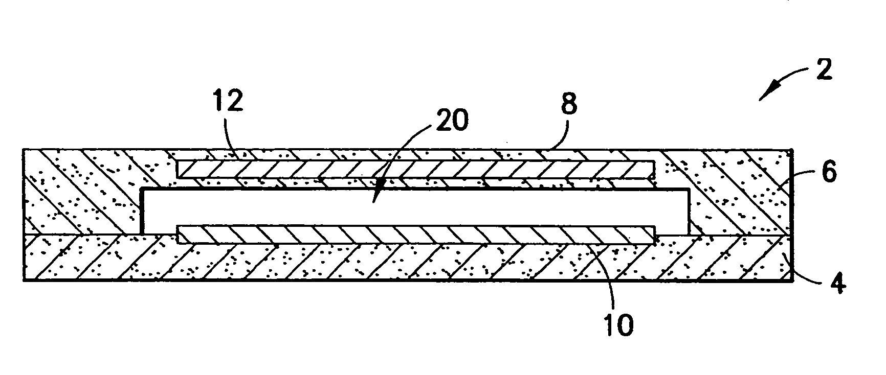
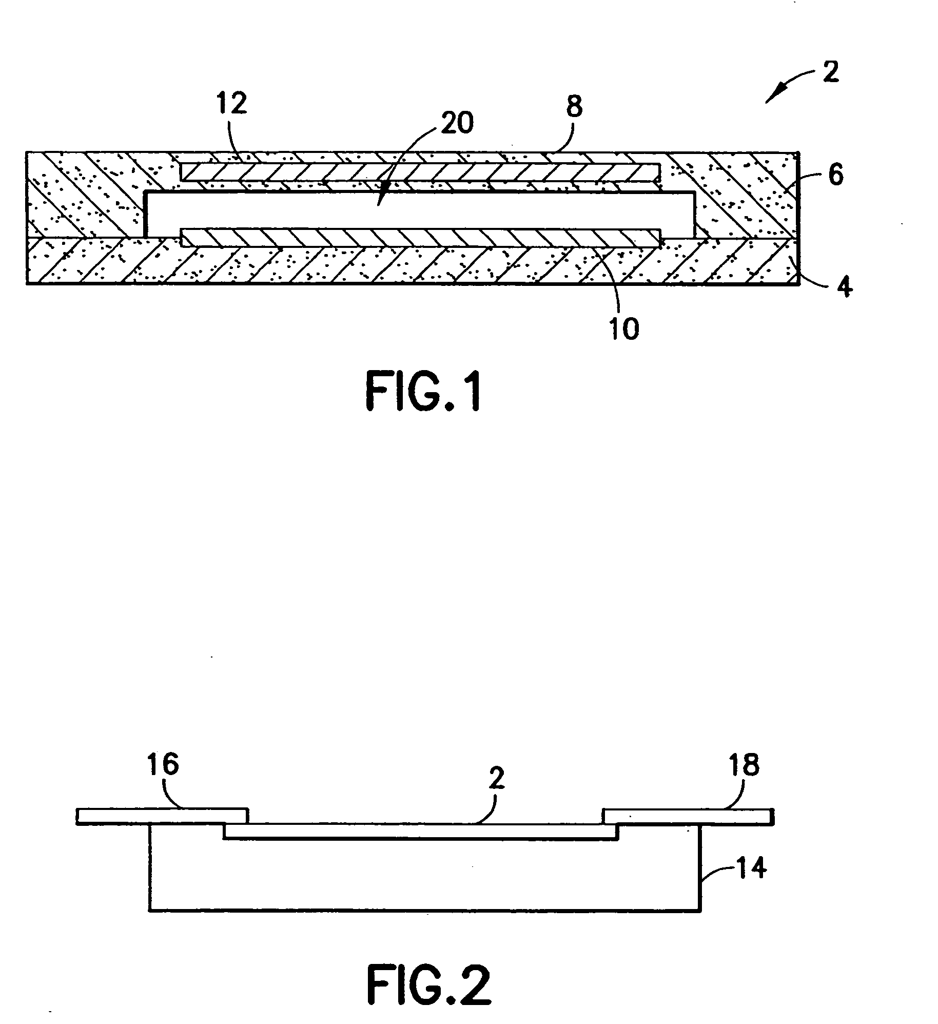
[0029] Referring to FIG. 1, a typical cMUT transducer cell 2 is shown in cross section. An array of such cMUT transducer cells is typically fabricated on a substrate 4, such as a silicon wafer. For each cMUT transducer cell, a thin membrane or diaphragm 8, which may be made of silicon nitride, is suspended above the substrate 4. The membrane 8 is supported on its periphery by an insulating support 6, which may be made of silicon oxide or silicon nitride. The cavity 20 between the membrane 8 and the substrate 4 may be air- or gas-filled or wholly or partially evacuated. A film or layer of conductive mater...


PUM

PropertyMeasurementUnit
mass percentaaaaaaaaaa
particle sizeaaaaaaaaaa

Abstract

An ultrasonic transducer device comprising: an ultrasonic transducer array micromachined on a substrate; flexible electrical connections connected to the transducer array; and a body of acoustically attenuative material that supports the substrate and the flexible electrical connections. The acoustic backing material may contain additional features, such as tabs or notches, for use in positioning the transducer on fixtures during manufacturing or positioning the transducer within a housing during final assembly. Tabs or other features that are used only during manufacturing may be subsequently removed from the device. The MUT device itself may also be thinned so as to provide flexibility as desired. The backing material is preferably matched in acoustic impedance to the silicon wafer so as to prevent reflection at the interface of any acoustic energy propagating rearward, i.e., in the direction away from the device front surface. The backing material may also possess a high thermal conductivity to assist in removal of heat from the device.

Description

BACKGROUND OF THE INVENTION [0001] This invention generally relates to micromachined ultrasonic transducers. In particular, the invention relates to capacitive micromachined ultrasonic transducers (cMUTs). One specific application for cMUTs is in medical diagnostic ultrasound imaging systems. [0002] Conventional ultrasound imaging transducers generate acoustic energy via a piezoelectric effect in which electrical energy is converted into acoustic energy using a poled piezoelectric ceramic material. The acoustic energy that is transmitted in the forward direction, which is in the direction of the patient being scanned, is coupled to the patient through one or more acoustic matching layers. However, the acoustic energy transmitted in the direction away from the patient being scanned is typically absorbed in and / or scattered in an acoustic backing material located on the backside of the transducer array. This prevents the acoustic energy from being reflected from structures or interfac...

Claims


Application Information

Patent Timeline
Patent Type & Authority Applications(United States)
IPC IPC(8): G01N29/24A61B8/00A61B8/14B06B1/02B06B1/06B81B3/00G01H11/06H01L41/053H01L41/08H01L41/09H01L41/187H01L41/193H02N2/00H04R1/32H04R17/00H04R19/00
CPCB06B1/0292B06B1/0685B06B1/0688Y10T29/49004Y10T29/49005Y10T29/4908G01H11/06
Inventor BAUMGARTNER, CHARLES E.MILLS, DAVID M.LEWANDOWSKI, ROBERT S.SMITH, LOWELL SCOTTWILDES, DOUGLAS G.
Owner GENERAL ELECTRIC CO
Why Eureka
Try Eureka