Protection circuit for semiconductor device and semiconductor device including the same

a protection circuit and semiconductor technology, applied in the direction of individual semiconductor device testing, circuit-breaking switches, instruments, etc., can solve the problems of difficult to readily realize such a protection circuit, difficult to form a precise model of the physical characteristics of the shielded line in the design process, etc., to improve the practical usefulness of the semiconductor device, improve the tamper resistance, and improve the effect of tamper resistan

Active Publication Date: 2005-03-03
PANASONIC SEMICON SOLUTIONS CO LTD
View PDF7 Cites 16 Cited by
  • Summary
  • Abstract
  • Description
  • Claims
  • Application Information

AI Technical Summary

Benefits of technology

[0008] An objective of the present invention is to provide a protection circuit having improved tamper resistance and a semiconductor device including such a protection circuit.
[0033] According to the present invention, a protection circuit with improved tamper resistance which has the function of detecting a tampering of the shielded line which covers a semiconductor device is readily realized. In a semiconductor device incorporating the protection circuit, confidential information stored in the semiconductor device is protected from fraudulent analysis means. Thus, a semiconductor device having an improved confidentiality protection function is readily provided.

Problems solved by technology

The above-described conventional technique is vulnerable to the fraudulent means for re-connecting partially-broken or peeled shielded line through a bypass that does not inhibit physical analysis by using appropriate means, such as a FIB processing technique, or the like, and the fraudulent means for externally connecting a conductive path as a bypass to a shielded line to disable the abnormality detecting function.
However, the physical characteristics of the shielded line are determined by the shape and the electric characteristic state of an underlying layer to be protected and, therefore, it is difficult to form a precise model of the physical characteristics of the shielded line in the designing process.
Additionally, because of an error in the production, a characteristic variation within a guaranteed operating environment, etc., it is difficult to readily realize such a protection circuit.

Method used


Image

  • Protection circuit for semiconductor device and semiconductor device including the same
  • Protection circuit for semiconductor device and semiconductor device including the same
  • Protection circuit for semiconductor device and semiconductor device including the same

Examples


embodiment 1

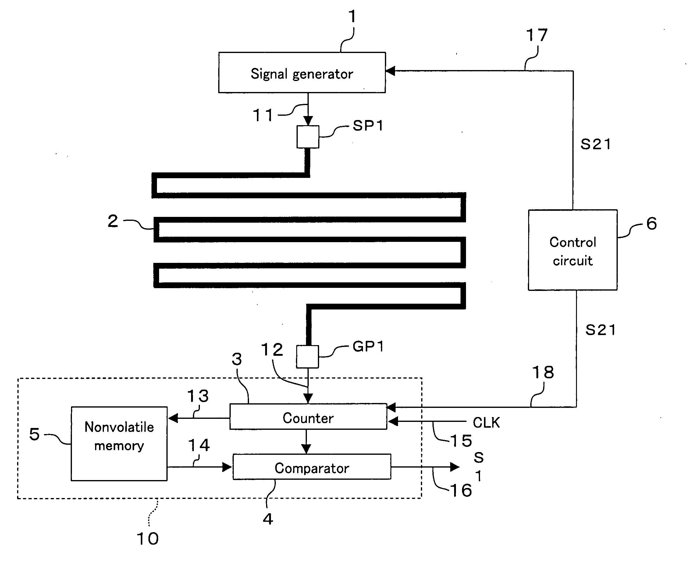
[0049]FIG. 1 shows the structure of a protection circuit according to embodiment 1. The protection circuit is incorporated in a semiconductor device for protecting confidential information stored in the semiconductor device from an analytic activity committed through fraudulent means. The protection circuit of embodiment 1 includes a signal generator 1, a shielded line 2, a control circuit 6 and a detector 10. The detector 10 includes a counter 3, a comparator 4 and a nonvolatile memory 5.

[0050] The shielded line 2 is the uppermost layer made of a metal in the production of a semiconductor device and is provided to cover a necessary and sufficient semiconductor device area to be protected (protection area). The shielded line 2 is arranged based on a unicursal topology to have only one course from a start point SP1 to an end point GP1. The control circuit 6 supplies control signal S21 to the signal generator 1 and the counter 3. In response to control signal S21 from the control cir...

embodiment 2

[0058]FIG. 6 shows the structure of a protection circuit according to embodiment 2. The protection circuit is incorporated in a semiconductor device for protecting confidential information stored in the semiconductor device from an analytic activity committed through fraudulent means. The protection circuit of embodiment 2 includes a signal generator 31, a shielded line pair (2a, 2b), and a detector 40. The detector 40 includes an operational amplifier 32, a reference voltage source 33 and a comparator 34.

[0059] The shielded line pair (2a, 2b) is the uppermost layer made of a metal and is provided to cover a necessary and sufficient semiconductor device area to be protected (protection area). The shielded lines 2a and 2b have the same shape and the same length. The shielded line 2a is arranged based on a unicursal topology to have only one course from a start point SP1a to an end point GP1a. The shielded line 2b is arranged based on a unicursal topology to have only one course from...

embodiment 3

[0065]FIG. 8 shows the structure of a protection circuit according to embodiment 3. The protection circuit is incorporated in a semiconductor device for protecting confidential information stored in the semiconductor device from an analytic activity committed through fraudulent means. The protection circuit of embodiment 3 includes a signal generator 51, a shielded line pair (2a, 2b), and a detector 60. The detector 60 includes a phase comparator 52, a filter circuit 53 and a determinator 54.

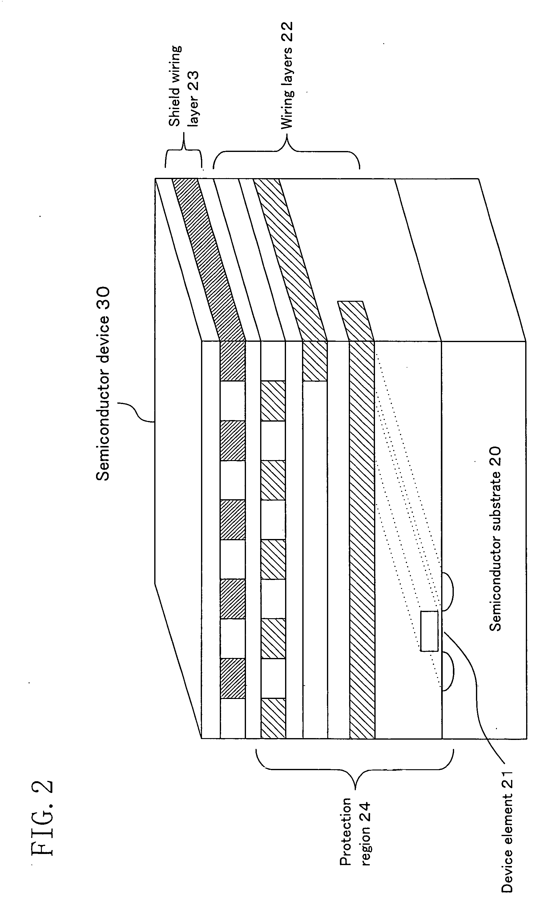
[0066] The cross-sectional structure of a semiconductor device incorporating the protection circuit of FIG. 8 is generally the same as that shown in FIG. 2. The shielded line pair (2a, 2b) shown in FIG. 8 is included in the shield wiring layer 23 and arranged so as to cover a protection region 24 (including the device element(s) 21 and the wiring layers 22). The circuit elements that constitute the signal generator 51, the phase comparator 52, the filter circuit 53 and the determinator 54 shown...


PUM


Abstract

A protection circuit comprises: at least one shielded line arranged to cover an area to be protected over a semiconductor device, the at least one shielded line having only one route from a start point to an end point; a signal generator for applying a signal to the start point of the shielded line; a counter which starts measurement of time in response to application of the signal to the start point of the shielded line by the signal generator and which ends measurement of the time in response to arrival of the signal at the end point of the shielded line; and a comparator for comparing the time measured by the counter with a reference value to output a fraud detection signal according to a result of the comparison.

Description

CROSS-REFERENCE TO RELATED APPLICATION [0001] This application claims priority under 35 U.S.C. §119(a) on Japanese Patent Application No. 2003-303823 filed on Aug. 28, 2003, the entire contents of which are hereby incorporated by reference. BACKGROUND OF THE INVENTION [0002] 1. Field of the Invention [0003] The present invention relates to a protection circuit for protecting confidential information stored in a semiconductor device from fraudulent analysis and to a semiconductor device including such a protection circuit. [0004] 2. Background Art [0005] In recent years, circuitry information and internal information of semiconductor devices require a considerably high level of confidentiality and secrecy. Especially in the field of IC cards, the safety of semiconductor devices is an essential feature and, therefore, it is necessary to protect important information from fraudulent analysis and prevent tampering and copying of internal information. In view of such, an increasing numbe...

Claims


Application Information

Patent Timeline
Patent Type & Authority Applications(United States)
IPC IPC(8): G06F21/00H01L27/04H01L21/822H01L23/58H04L9/10
CPCG06F21/87H01L23/576H01L2924/0002H01L2924/00
Inventor MATSUNO, NORIAKI
Owner PANASONIC SEMICON SOLUTIONS CO LTD
Why Eureka
Try Eureka