Resistor element, stress sensor and method for manufacturing them

a technology of resistor elements and stress sensors, applied in the direction of instruments, conductive pattern formation, force/torque/work measurement apparatus, etc., can solve problems such as problems, difficulties in the former to form resistors, and different from the conventional technique described above, so as to reduce the variation in the effect of decreasing the resistance of the resistor element 8

Inactive Publication Date: 2005-03-10
ELAN MICROELECTRONICS CORPORATION
View PDF13 Cites 18 Cited by
  • Summary
  • Abstract
  • Description
  • Claims
  • Application Information

AI Technical Summary

Benefits of technology

[0092] Since the resistor element 8 of the present invention has the second structure, an exuded part 14 shown in FIG. 12 (a) generated in the past can be reduced, and hence the variation in resistance of the resistor element 8 can be decreased. Since the exuded part 14 is formed of the resistor 2, is brought into contact with the circuit pattern electrode 1, and is electrically connected to the opposing electrode, the resistance of the resistor element 8 is influenced. The degree of the influence is an uncertain factor depending on the amount of the exuded part 14, the shape thereof, and the like. The reason for this is that it is very difficult to control the amount of the exuded part 14 and the shape thereof as described above. Hence, by eliminating the uncertain factor as is the structure described above of the present invention, even in the resistor element 8 comprising the electrodes composed of the parts of the conductors 9 on the surface of the insulating board 3 obtained as the remains by partly removing the conductor layer on the surface, and the resistor 2 provided by film formation between the pair of the electrodes on the surface of the insulating board 3, the variation in resistance of the resistor element 8

Problems solved by technology

However, when the insulating board for a stress sensor is an insulating board having conductors which are obtained by partly removing a conductive layer on a surface as remains, and when the stress sensor uses parts of the conductors 9 as electrodes and resistor elements as a strain gage, each element formed of a resistor provided between a respective pair of the electrodes on the surface of the insulating board, a problem different from that of the conventional technique described above may arise.
In the past, the electrodes (conductors) constituting the resistor elements were formed by a screen printing method, and in the above technique, the conductors are formed of the remains obtained by partly removing the conductor layer on the surface; hence, the problem is generated by the difference described above.
The reason for this is that it is difficult for the former to form a resistor 2 having a uniform shape.
Although the resistances are equal to each other, when the trimming lengths are extremely different from each other as described above, due to the change in ambient environment, particularly an ambient temperature, the resistance stability cannot be obtained.
In addition, in a stress sensor i

Method used


Image

  • Resistor element, stress sensor and method for manufacturing them
  • Resistor element, stress sensor and method for manufacturing them
  • Resistor element, stress sensor and method for manufacturing them

Examples


Embodiment Construction

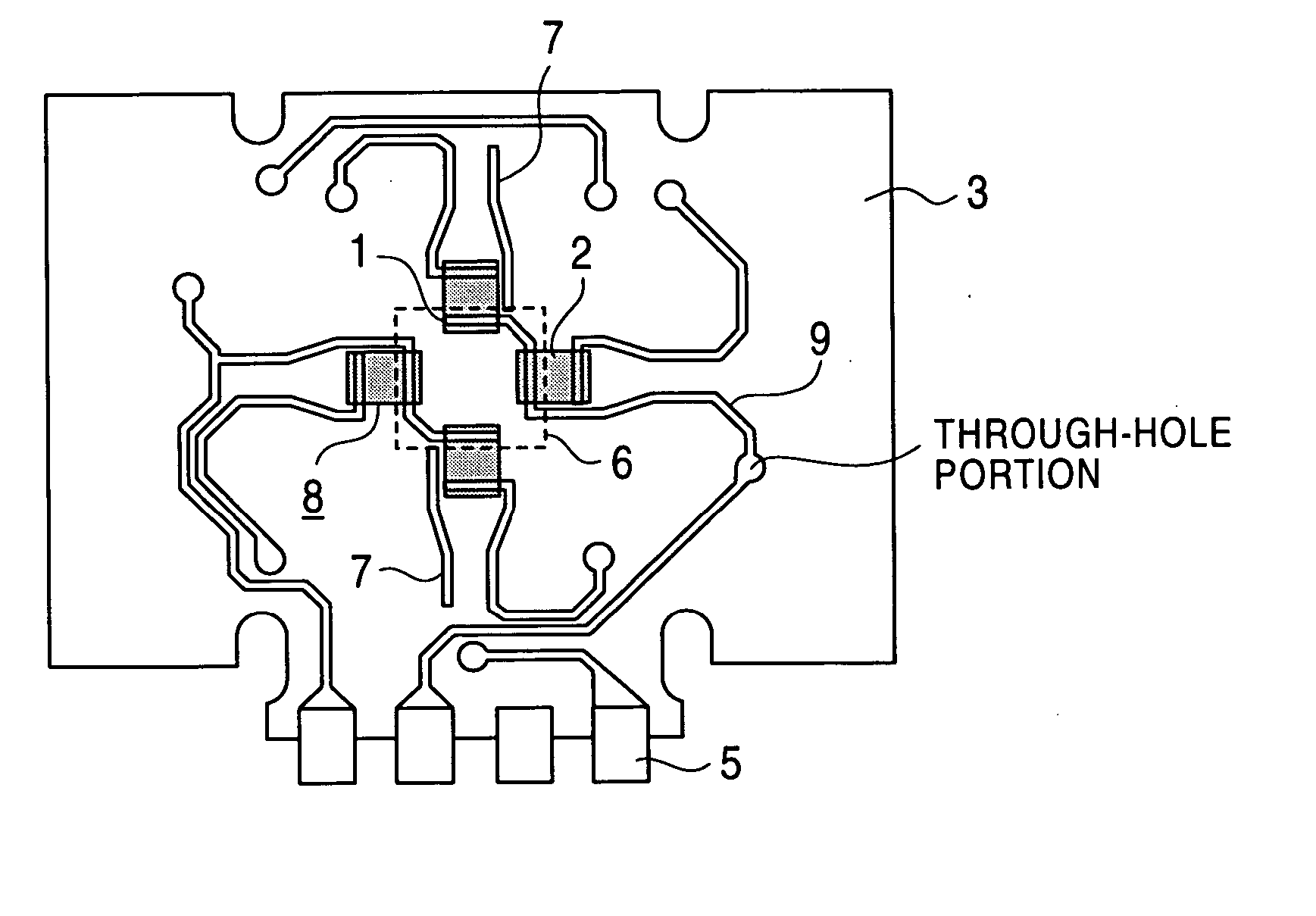
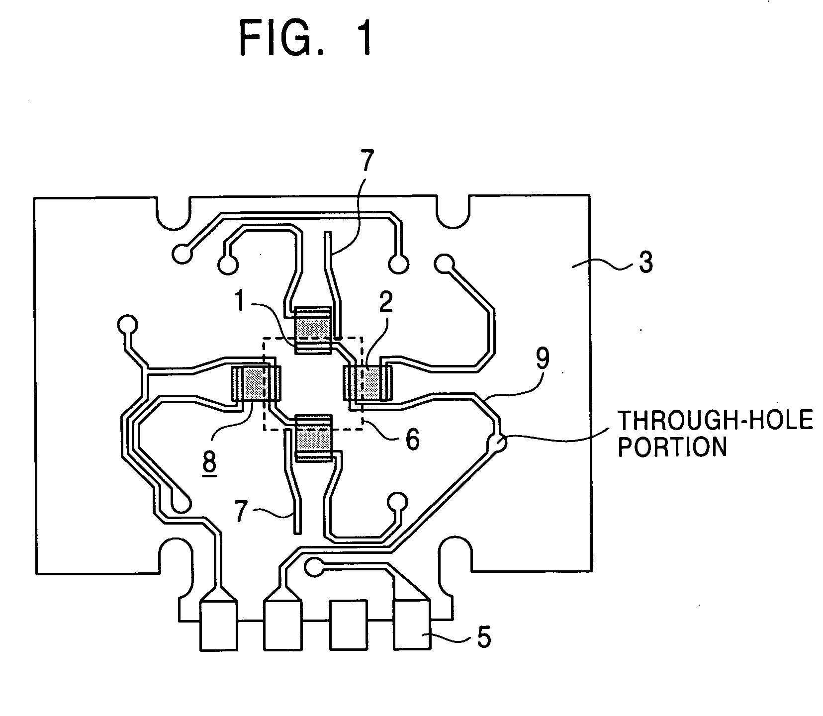
[0116] Hereinafter, with reference to figures, an example of embodiments of stress sensors having structures 1a to 1d according to the present invention will be described, the stress sensor having a molded body of a glass fiber filled epoxy resin as a board (1.2 mm thick).

[0117] First, after copper foils 18 μm thick are adhered to both surfaces of an insulating board 3, known etching treatment is performed for the copper foils except for necessary portions thereof, thereby forming conductors 9, resistor-element electrodes (circuit pattern electrodes 1), and board terminal parts 5. A layout of the conductors 9 and resistor-element electrodes on a surface of the insulating board 3 of one stress sensor thus formed is shown in FIG. 1. In this case, the side at which the resistor elements are formed is only shown; however wires made of conductors are also provided on the rear surface of this insulating board 3.

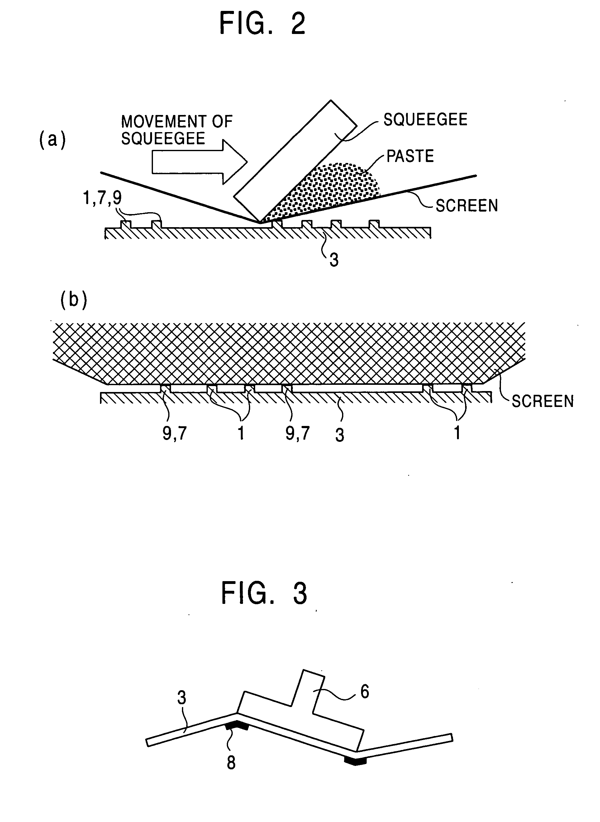
[0118] On the surface of the insulating board 3, the conductors 9 (printing ...


PUM

PropertyMeasurementUnit
Electrical resistanceaaaaaaaaaa
Electrical conductoraaaaaaaaaa
Widthaaaaaaaaaa

Abstract

A stress sensor in which the direction and magnitude of a stress being applied to a post (6) bonded to or integrated with the surface of an insulating board (3) can be grasped from variation in the resistance of a plurality of resistor elements (8) being stimulated by application of the stress while suppressing variation in the shape of each resistor (2). The resistor element (8) comprises a resistor (4) formed, by screen print, between a pair of electrodes for the resistor element, i.e. circuit pattern electrodes (1), arranged on the surface of the insulating board (3). The electrode is connected, through a conductor (9), with a board terminal part (5) arranged at one end of the insulating board (3). The electrode (1) and the conductor (9) or a print accuracy adjusting member (7) have a constant height from the surface of the insulating board (3). Arrangement of the conductor (9), the electrode (1) and the print accuracy adjusting member (7) is entirely identical or similar for the plurality of resistor elements (8) in the vicinity thereof.

Description

TECHNICAL FIELD [0001] The present invention relates to resistor elements and stress sensors as one application filed thereof, which can be used, for example, for a pointing device for personal computers or a multifunctional and multidirectional switch for various electronic devices. BACKGROUND ART [0002] A stress sensor has been disclosed in Japanese Unexamined Patent Application Publication No. 2000-267803, which is capable of grasping the direction and magnitude of a stress applied to a post bonded to or integrated with a surface of an insulating board from variation in resistance of a plurality of resistor elements caused by stimulation provided thereto resulting form the application of the stress to the post. The formation of the resistor elements thus disclosed, which elements form a strain gage, is performed by screen printing of all constituent elements of the resistor elements on a surface of a ceramic board. [0003] The structure is formed as shown in FIG. 15, in which four...

Claims


Application Information

Patent Timeline
IPC IPC(8): G01L1/22G01L5/16G01L5/22H01C10/10H01C13/02H01C17/065H05K1/09H05K1/16H05K3/12
CPCG01L1/2287G01L5/162H01C10/103H01C13/02H01C17/065Y10T29/49103H05K1/167H05K3/1216H05K2201/09781H05K2203/1453H05K1/095
Inventor OOBA, ETSUOINUKAI, ATSUOMIKARASAWA, FUMIAKIYAJMA, HIROSHI
Owner ELAN MICROELECTRONICS CORPORATION
Why Eureka
Try Eureka