

Method for producing display - device
a display device and passive matrix technology, applied in semiconductor devices, instruments, optics, etc., can solve the problems of easy disconnection of electrical wiring, and achieve the effect of improving reliability and durability of the liquid crystal display devi
- Summary
- Abstract
- Description
- Claims
- Application Information
AI Technical Summary
Benefits of technology
Problems solved by technology
Method used
Image

Examples
embodiment 1
[0069] [Embodiment 1]
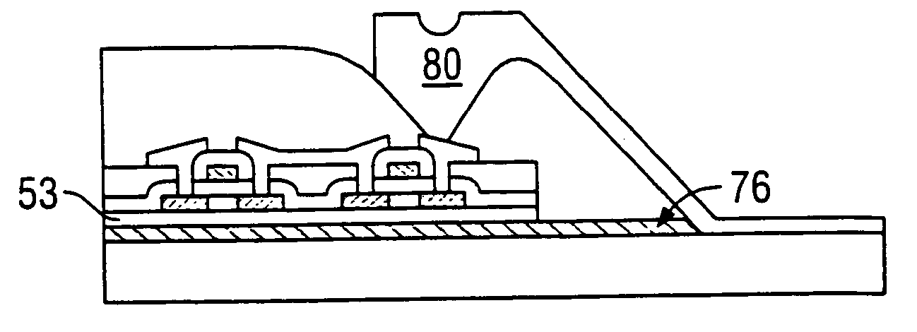
[0070] The embodiment shows a schematic producing process for one substrate in a passive matrix type liquid crystal display device, using FIGS. 4A to 5D. FIGS. 4A to 4C show a schematic process for forming a driver circuit on a stick crystal, and FIGS. 5A to 5D show a schematic process for forming the driver circuit on a substrate in a liquid crystal display device.
[0071] A silicon film having a thickness of 3000 Å is deposited as a peeling layer 51 on a glass substrate 50. Since this silicon film is etched when a circuit formed thereon is peeled from the substrate, there is no problem almost with respect to a film quality, so that the silicon film may be deposited by a method that mass-production is possible. The silicon film may be amorphous or crystalline and include another element.
[0072] As the glass substrate, a glass (containing no alkali or alkali at a low concentration) or a quartz glass such as Corning 7059, Corning 1737, NH technoglass NA 45, NH tec...
embodiment 2
[0084] [Embodiment 2]
[0085] The embodiment shows a schematic process for producing a semiconductor integrated circuit on a stick crystal. The embodiment will be explained using FIGS. 6A and 6B.
[0086] In FIG. 6A, a peeling layer 102 made of silicon is formed on a substrate 101, and then a driver circuit (a semiconductor integrated circuit) 100 having TFTs is formed on the peeling layer 102. These are formed by the same process as in Embodiment 1. A silicon oxide film is formed as a passivation film. In the embodiment, two-layer silicon oxide films 103 and 104 are formed by plasma CVD. The first silicon oxide film 103 is formed by applying a relatively high power, and the second silicon oxide film 104 is formed by a relatively low power. A thickness of the first silicon oxide film 103 is 100 to 500 nm, and a thickness of the second silicon oxide film 104 is 500 to 1000 nm.
[0087] After a resist 105 for patterning is formed, the substrate having a laminate is immersed in a {fraction (...
embodiment 4
[0106] [Embodiment 4]
[0107] The embodiment shows a schematic process for electrically connecting a wiring on a substrate of a liquid crystal display device to a metal wiring in a semiconductor integrated circuit using FIGS. 11A and 11B. FIGS. 11A and 11B are magnification views of a connection portion of a wiring electrode on a substrate of a liquid crystal display device and a metal wiring of a semiconductor integrated circuit.
[0108] A wiring electrode 201 made of a transparent conductive film is formed on a substrate 200 of a liquid crystal display device by sputtering. Further, a pad 202 made of a metal having a low melting point is formed in a portion to be electrically connected to a semiconductor integrated circuit by sputtering.
[0109] Using the method as described in Embodiment 1, a semiconductor integrated circuit and a metal wiring which are formed on another substrate 203 are fixed mechanically through an adhesive 204. (FIG. 11A)
[0110] An overlapping portion of the meta...
PUM
| Property | Measurement | Unit |
|---|---|---|
| width | aaaaa | aaaaa |
| thickness | aaaaa | aaaaa |
| thickness | aaaaa | aaaaa |
Abstract
Description
Claims
Application Information