
Method for manufacturing optical recording medium

Inactive Publication Date: 2005-03-10
TDK CORPARATION
View PDF1 Cites 0 Cited by
  • Summary
  • Abstract
  • Description
  • Claims
  • Application Information

AI Technical Summary

Benefits of technology

[0017] In view of the foregoing problems, various exemplary embodiments of this invention provide a method for manufacturing an optical recording medium that can suppress the amount of eccentricity of a center hole to be small and can form a light transmitting layer in a region surrounding the central hole to be a uniform thickness.
[0026] According to the exemplary embodiment of this invention, since the manufacturing hole is formed in the substrate, it is easy to transfer and store the substrate in a manufacturing process. Moreover, since the substrate can be positioned by using the manufacturing hole as a reference, the amount of eccentricity of the central hole can be suppressed to be small. In addition, since the radiation curable resin is supplied to the region surrounding the manufacturing hole that has a smaller inner diameter than the central hole (surrounding the core member that comes into close contact with the inner circumference of the manufacturing hole), the light transmitting layer can be spread and formed with a uniform thickness. Even if a flash is generated around the core member or the light transmitting layer peels off in the region surrounding the manufacturing hole when the core member is removed, the flash or the region in which the light transmitting layer peeled off is removed because the central hole having a larger inner diameter than that of the manufacturing hole. Therefore, it is possible to surely form the light transmitting layer having a uniform thickness even in the region surrounding the central hole.

Problems solved by technology

On the other hand, there is a tendency that precision of recording or reproducing the information is degraded as the wavelength of the illumination light becomes shorter and the numerical aperture of the lens becomes larger.
However, the light transmitting layer having a thickness of 0.6 mm cannot provide sufficient stiffness and strength by itself to DVD.
However, when the spin-coating method is adopted to a substrate having a central hole formed therein, the thickness of the light transmitting layer is liable to become uneven.
Thus, the recording and reproducing of the information with high density may be difficult to perform.
Thus, it takes a longer time to run out the resin there.
Therefore, the thickness of the resultant layer does not become uniform.
It is practically impossible to perform such control.
However, the substrate having no central hole is difficult to transfer, store and the like, in the manufacturing process of the optical recording medium and therefore decreases the production efficiency.
Moreover, it is difficult to position the substrate having no central hole with high precision.
In addition, when the central hole is formed, the amount of eccentricity of the central hole with respect to grooves or pits may become large.
Thus, the light transmitting layer cannot be formed in the region surrounding the central hole.
Moreover, when the blocking member is removed from the substrate, an inner circumferential edge of the light transmitting layer may be damaged.
For example, when the blocking member is removed from the substrate by being moved up before irradiation of UV rays or the like, the resin may become thready or the like, thus spoiling the appearance of the inner circumferential edge of the light transmitting layer.
On the other hand, when the blocking member is removed from the substrate by being moved up after irradiation of UV rays or the like, the blocking member may not be easily separated from the substrate because the resin surrounding the blocking member is cured and causes the blocking member to adhere to the substrate.

Method used


Image

  • Method for manufacturing optical recording medium
  • Method for manufacturing optical recording medium
  • Method for manufacturing optical recording medium

Examples


examples

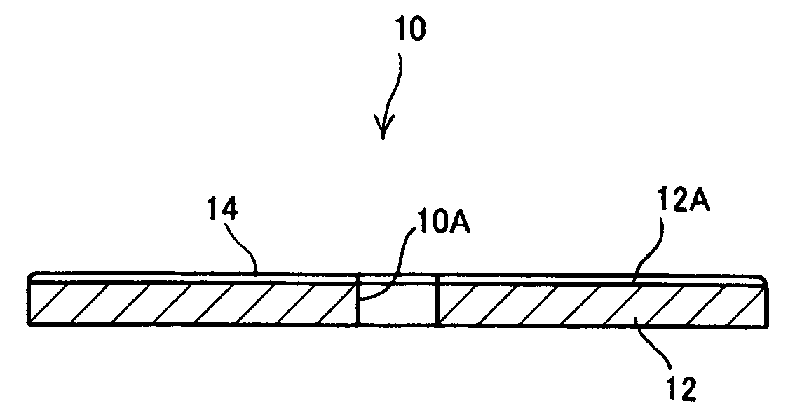
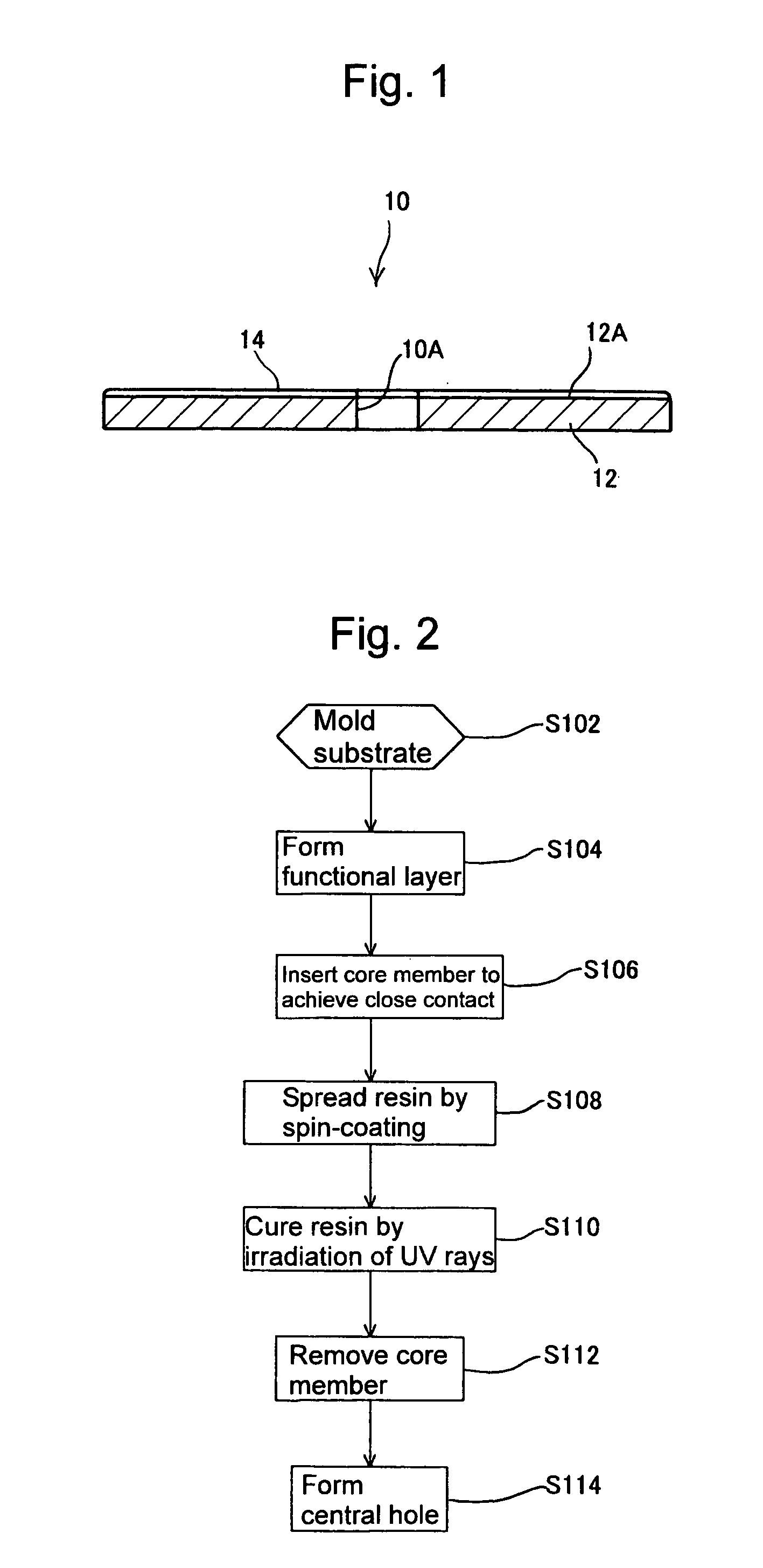
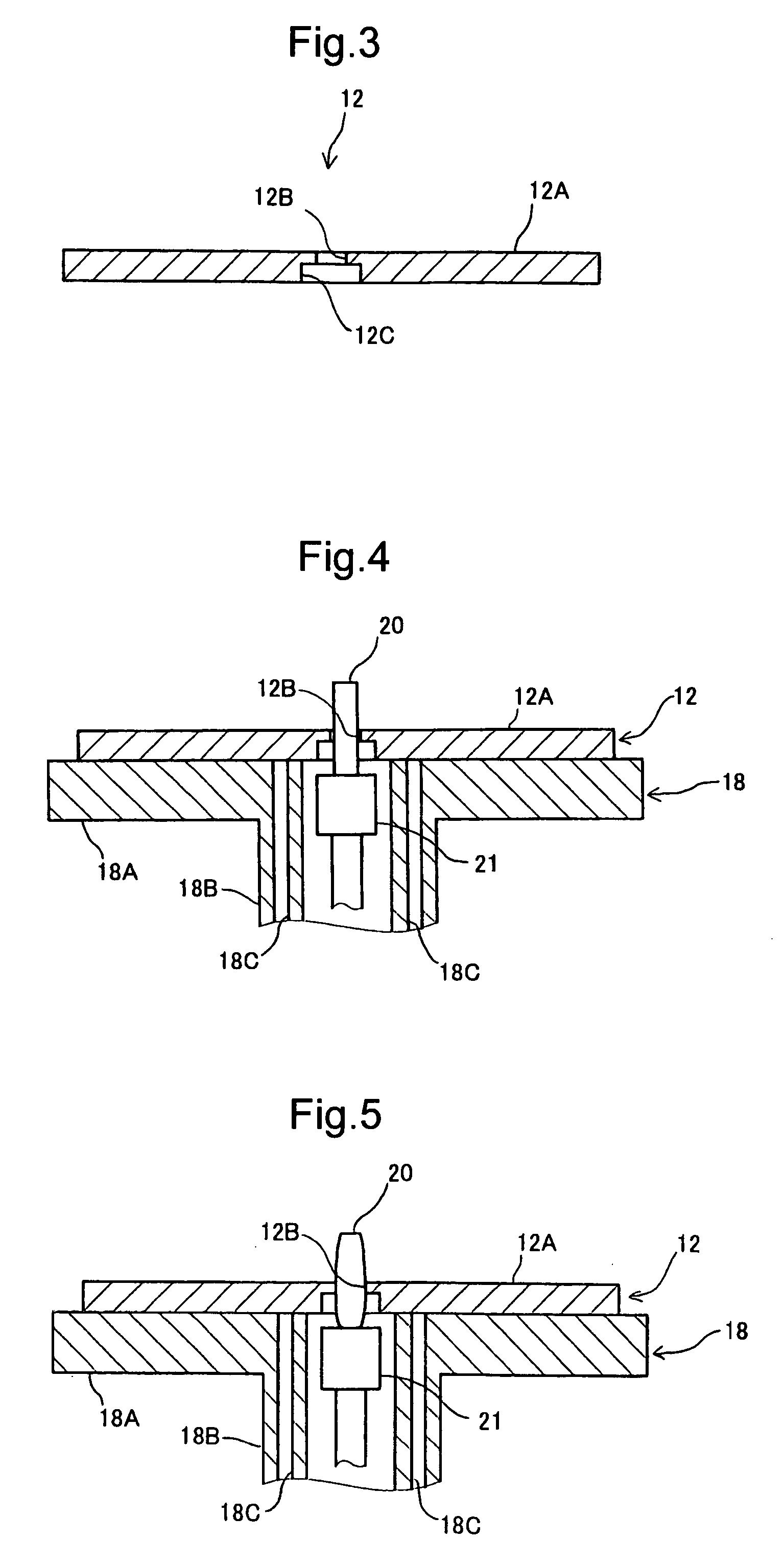
[0065] In a manner described in the above exemplary embodiment, ten substrates 12 were molded for each of respective 10 inner diameters of the manufacturing hole 12B, i.e., 2 mm, 4 mm, 5 mm, 6 mm, 7 mm, 8 mm, 9 mm, 10 mm, 12 mm and 14 mm, so that a total of 100 substrates 12 were molded. For each substrate 12, a resin was spread on the information recording surface 12A of the substrate 12 under a condition of spin-coating in which revolutions per minute of the turntable 18 was approximately 2000 rpm. Then, the resin was exposed to UV rays, thereby being cured to form a light transmitting layer 14. In this manner, 100 optical recording media 10 were fabricated. In this manufacturing, the following materials were used for the light transmitting layer 14.

ART RESIN ® UN-5200 (manufactured by Negami77wt %Chemical Industrial Co., Ltd.):ARONIX ® M-315 (manufactured by Toagosei10wt %Co., Ltd.):THF-A (manufactured by Kyoeisha Chemical Co., Ltd.):10wt %Irgacure ® 184 (manufactured by Ciba S...


PUM

PropertyMeasurementUnit
Diameteraaaaaaaaaa
Diameteraaaaaaaaaa
Diameteraaaaaaaaaa

Abstract

A method for manufacturing an optical recording medium is provided, which can suppress the amount of eccentricity of a central hole to be small and can form a light transmitting layer with a uniform thickness even in a region around the central hole. In this manufacturing method, a manufacturing hole having a smaller inner diameter than that of the central hole is formed in a substrate. A core member is fitted into the manufacturing hole to be in close contact with the inner circumference of the manufacturing hole. A light transmitting layer is spread over an information recording surface of the substrate by supplying radiation curable resin in a region around the core member and rotating the substrate. Then, the light transmitting layer is cured by irradiation of radiation, and the core member is removed from the manufacturing hole. Thereafter the central hole is formed.

Description

BACKGROUND OF THE INVENTION [0001] 1. Field of the Invention [0002] The present invention relates to a method for manufacturing an optical recording medium in which a light transmitting layer is formed on a side of a substrate, which is a side closer to an information recording surface, so as to be thinner than the substrate. [0003] 2. Description of the Related Art [0004] In recent years, optical recording media such as CDs (Compact Disc), DVDs (Digital Versatile Disc), and the like, have spread rapidly. Typical optical media have an outer diameter of 120 mm and a thickness of 1.2 mm that are standardized. For a DVD, laser light having a shorter wavelength than that for a CD is used as illumination light and numerical aperture of a lens for the illumination light is made larger than that for a CD. Thus, s DVD enables the larger amount of information to be recorded and reproduced with higher density, as compared with CDs. [0005] On the other hand, there is a tendency that precision ...

Claims


Application Information

Patent Timeline
IPC IPC(8): B29C33/00B29C35/08B29C41/04B29C41/20B29C41/40B29D17/00G11B7/26
CPCB29C33/0033B29C41/045B29C41/20G11B7/266B29C2035/0827B29D17/005B29L2017/005B29C41/40
Inventor KOMAKI, TSUYOSHI
Owner TDK CORPARATION
Features
  • Generate Ideas
  • Intellectual Property
  • Life Sciences
  • Materials
  • Tech Scout
  • Unparalleled Data Quality
  • Higher Quality Content
  • 60% Fewer Hallucinations
Learn More