

Method of manufacturing an OLED
- Summary
- Abstract
- Description
- Claims
- Application Information
AI Technical Summary
Benefits of technology
Problems solved by technology
Method used
Image

Examples
first embodiment
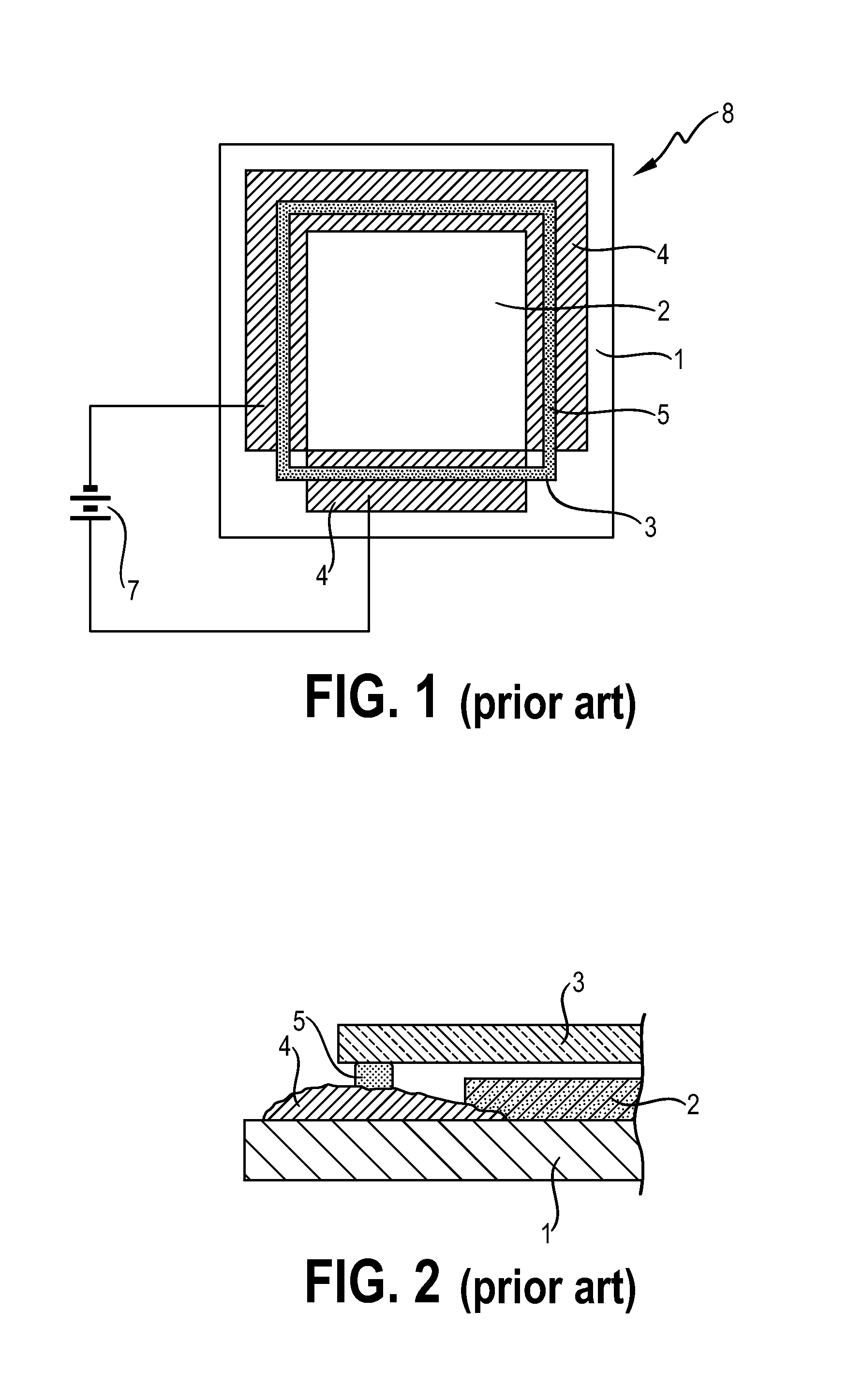
[0033]FIG. 4 shows a cross-section of an outer region of an OLED device obtained using the method according to the invention, in which the conductive protective layer 6 is applied on the outer region of the contact pad 4. To encapsulate the OLED, an adhesive 5 is applied along the border between the conductive protective layer 6 and the exposed contact pad 4. Of course, the adhesive 5 could be applied to lie just inside the edge of the conductive protective layer 6, without touching the contact pad surface. The cover lid 3 is then put into place and the exposed contact pad 4, i.e. the surface not covered by the conductive protective layer 6, is effectively protected from the corrosive effects of the atmosphere.
second embodiment
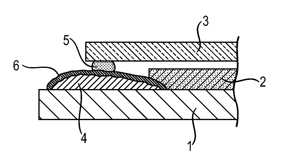
[0034]FIG. 5 shows a cross-section of an outer region of an OLED device obtained using the method according to the invention, in which the conductive protective layer 6 is applied to cover the entire contact pad 4, and the adhesive is applied onto the conductive protective layer 6.
third embodiment
[0035]FIG. 6 shows a cross-section of an outer region of an OLED device obtained using the method according to the invention, in which the contact pad 4 is narrower than in the realisations described above. Here, the conductive protective layer 6 is applied adjacent to the narrow contact pad 4, and the adhesive 5 is applied along the border between the conductive protective layer 6 and the contact pad 4.
[0036]The contact pads can be isolated using any combination of the techniques described above. For example, the realisation of FIG. 4 could be used for the larger contact pad (often the cathode), while the shorter contact pad could be realised as shown in FIG. 6. The realisation shown in FIG. 5 might be preferred on account of its straightforwardness. The realisation of FIG. 4 might be preferred since it combines a low material consumption with an optimal isolation from the harmful effects of the environment and in no way detracts from the conductivity of the contact pads.
[0037]FIG....
PUM
 Abstract
Description
Claims
Application Information