Light-emitting device with enlarged active light-emitting region

a technology of active light and light-emitting region, which is applied in the direction of solid-state devices, semiconductor devices, television systems, etc., can solve the problems of shortening affecting the luminous yield and luminance of the device, and affecting the service life of the device. , to achieve the effect of enhancing the luminous yield and luminan

Inactive Publication Date: 2005-03-17
OPTO TECH
View PDF3 Cites 140 Cited by
  • Summary
  • Abstract
  • Description
  • Claims
  • Application Information

AI Technical Summary

Benefits of technology

[0017] Accordingly, it is the key point of the present invention to provide a novel light-emitting device, not only enhancing the luminous yield and luminance by means of an effectively unifo

Problems solved by technology

Not only shortening the service life of the device, but also unsuitable for the high power light-emitting device may take place, owing to the high working temperature concentration in a certain area, because the part of PN junction 137 is removed to narrow the active light-emitting region, correspondingly.
Not only shortening the service life of the device, but also unsuitable for the high power light-emitting device may t

Method used


Image

  • Light-emitting device with enlarged active light-emitting region
  • Light-emitting device with enlarged active light-emitting region
  • Light-emitting device with enlarged active light-emitting region

Examples


Embodiment Construction

[0042] The structural features and the effects to be achieved may further be understood and appreciated by reference to the presently preferred embodiments together with the detailed description.

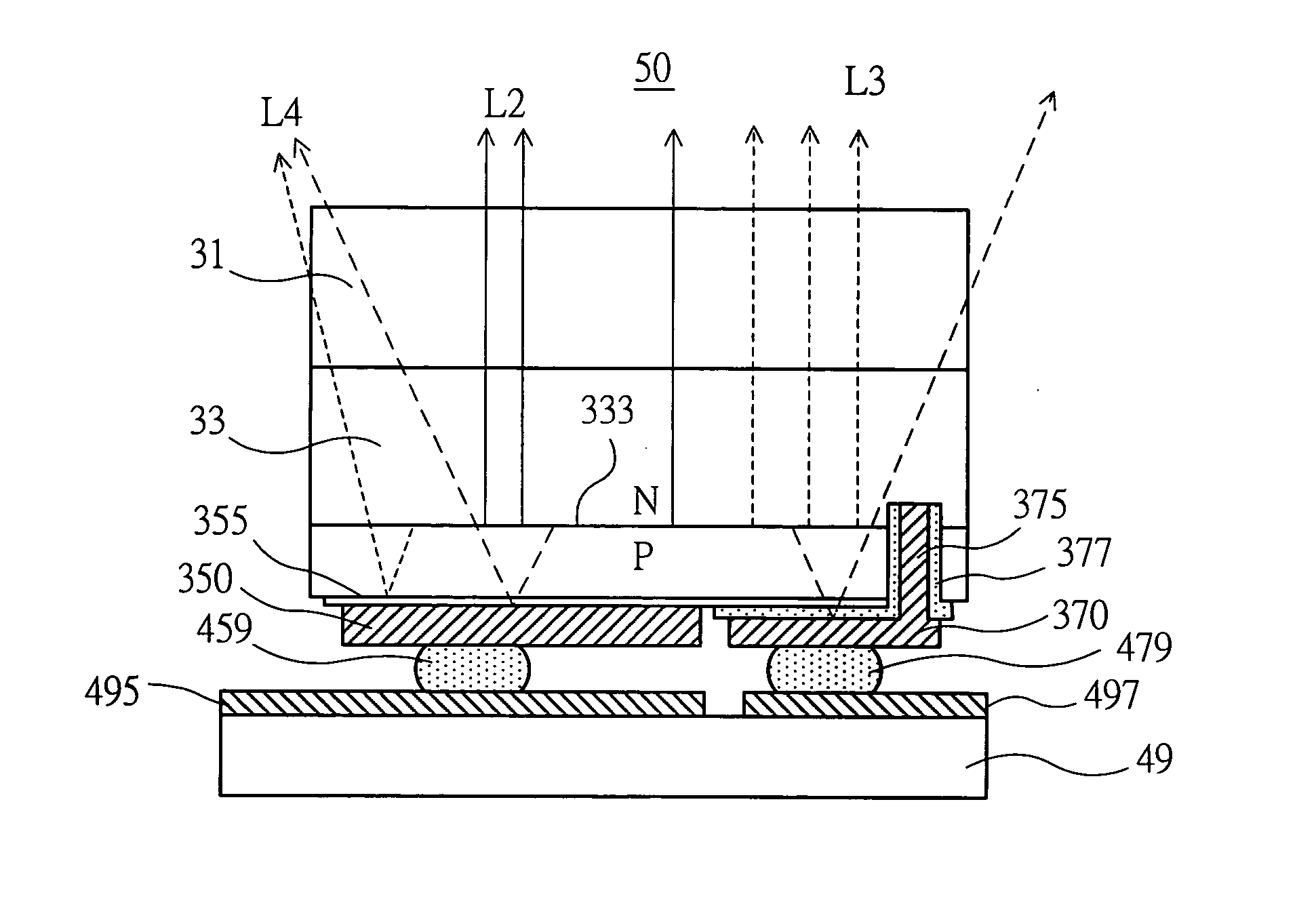
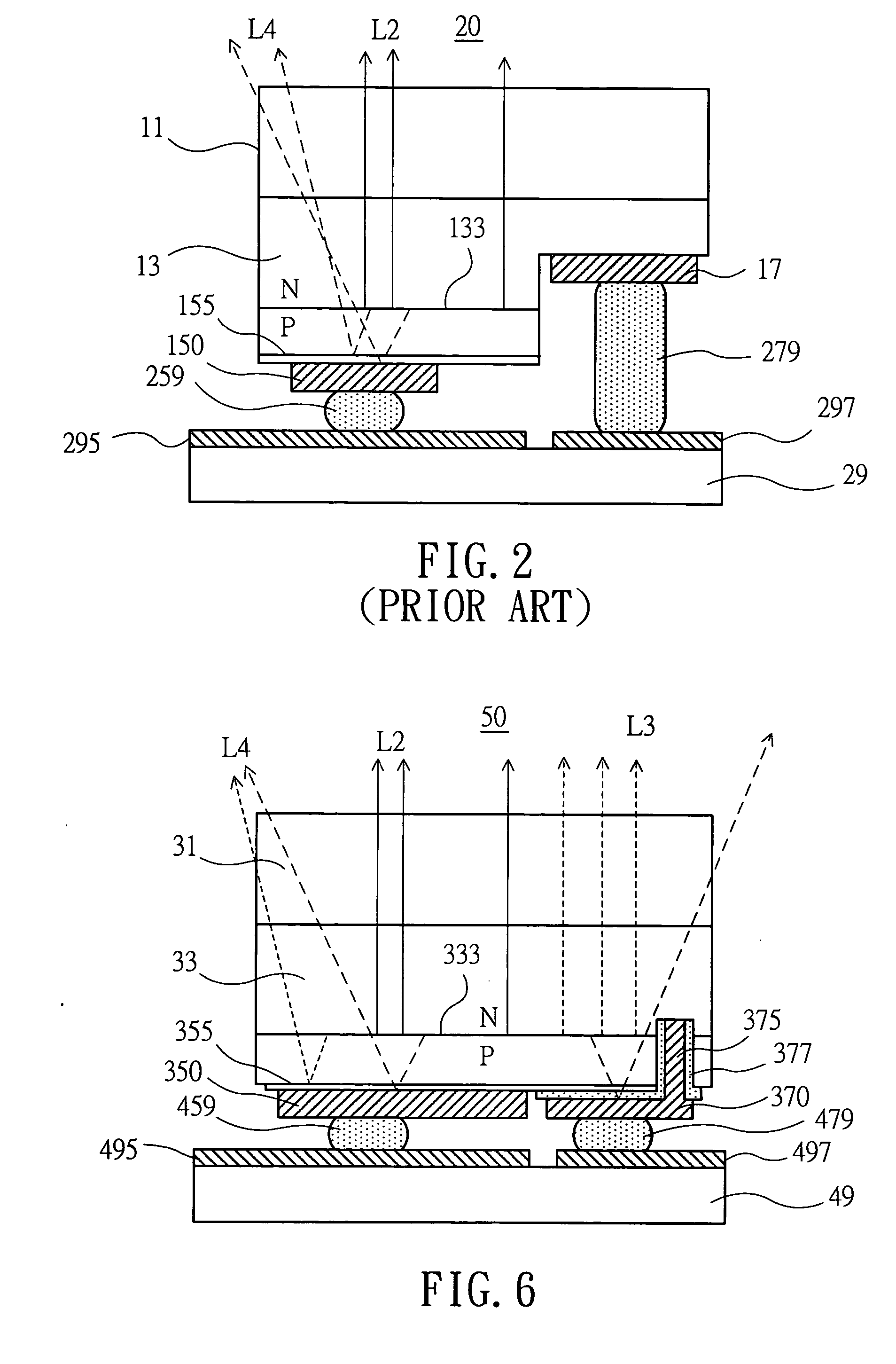
[0043] Firstly, referring to FIGS. 3A and 3B, there are shown a structural cross section view and a top view, respectively, according to one preferred embodiment of the present invention. As shown in these figures, a light-emitting device (LED) 30 of the present invention mainly comprises a LED substrate 31 formed thereon with an epitaxial layer 33, composed of a first material layer 331 and a second material layer 335 in turn. The first material layer 331 is formed onto the top surface of the LED substrate 31, and it is followed by forming the second material layer 335 onto the former, in such a way that a PN junction or light-emitting region is formed between the first material 331 and the second material 335 naturally. Thus, a flat light-emitting diode is completed. At an appropriate pos...


PUM


Abstract

A light-emitting device is provided. The device is with an enlarged active light-emitting region, mainly comprising a LED substrate provided with a first material layer and a second material layer on the top surface thereof in turn, and a PN junction formed between the first material layer and the second material layer naturally. Moreover, a first extended trench, allowed for passing through the second material layer and a part of the first material layer, is provided, and a first extended electrode is disposed inside the first extended trench. The electrical connection between the first extended electrode and the first electrode disposed on one part of top surface of the second material layer is made, such that the first electrode may be located at a horizontal level approximately identical to that of a second electrode equally disposed at the other part of top surface of the second material. Thus, it is possible for not only facilitating the following fabrication process, but also enlarging the active light-emitting region of the PN junction, due to the fact that a removed part of the second material layer for the formation of the first electrode required in the conventional light-emitting device is not necessary. Thereby, an effectively enhanced luminance and a prolonged service life are achieved.

Description

FIELD OF THE INVENTION [0001] The present invention is related to a light-emitting device, particularly to a light-emitting device with an enlarged active light-emitting region for effectively enhancing the luminance (brightness) and prolonging the service life thereof. BACKGROUND [0002] Light-emitting diodes (LEDs) have been widely used in various products, such as indicating lights, advertisement panels, traffic signal lights, vehicle lamps, display panels, communication instruments, consumer electronics, and so on, owing to features and merits including long service life, small volume, low heat, low power consumption, high response speed, no radiation, and monochromatic light. [0003] Accordingly, for the conventional light-emitting device, such as a flat light-emitting diode shown in FIGS. 1A and 1B, a light-emitting device 10 mainly comprises a LED substrate 11 formed with a first material layer 131 and a second material layer 135, in turn, thereon. The first material layer 131 ...

Claims


Application Information

Patent Timeline
IPC IPC(8): H01L27/15H01L33/42H01L33/50H01L33/62
CPCH01L33/382H01L2224/13H01L33/405H01L2224/05009H01L2224/13025H01L2224/05568H01L2224/05023H01L2224/05001H01L2924/00014H01L24/05H01L24/06H01L2224/06102H01L2224/1703H01L2224/05599H01L2224/05099H04M1/04H02J7/0042H04N5/655
Inventor LIN, MING-DERHSU, JUNG-KUEILIN, SAN-BAO
Owner OPTO TECH
Why Eureka
Try Eureka