
Electrical circuit assembly with improved shock resistance

a technology of electrical circuit and shock resistance, which is applied in the direction of sustainable manufacturing/processing, final product manufacturing, semiconductor/solid-state device details, etc., can solve the problems of time-consuming and costly rework of the connection holding the circuit device to the substrate, and the full benefits of using a chip package rather than a microchip directly attached to the circuit board are not realized. , to achieve the effect of reducing assembly tim

Inactive Publication Date: 2005-03-17
COOKSON ELECTRONICS INC
View PDF66 Cites 22 Cited by
  • Summary
  • Abstract
  • Description
  • Claims
  • Application Information

AI Technical Summary

Benefits of technology

[0005] Among the several objects of this invention may be noted the provision of an assembly which includes a releasable mechanical connection between an integrated circuit device and a substrate; the provision of such an assembly which allows economical manufacture; the provisions of such an assembly which permits simple testing; the provision of such an assembly which reduces assembly time; the provisions of such an assembly which provides a reliable electrical and mechanical connection; and the provision of such an assembly that allows easy removal and replacement of the integrated circuit device.

Problems solved by technology

Since underfill is a thermoset polymer that cannot be softened by heating, rework of the connection holding the circuit device to the substrate is time consuming and costly.
By using underfill to attach a chip package to a circuit board, the full benefits of using a chip package rather than a microchip directly attached to the circuit board are not realized because chip attachments using underfill are considered permanent connections that cannot readily be released.

Method used


Image

  • Electrical circuit assembly with improved shock resistance
  • Electrical circuit assembly with improved shock resistance
  • Electrical circuit assembly with improved shock resistance

Examples


Embodiment Construction

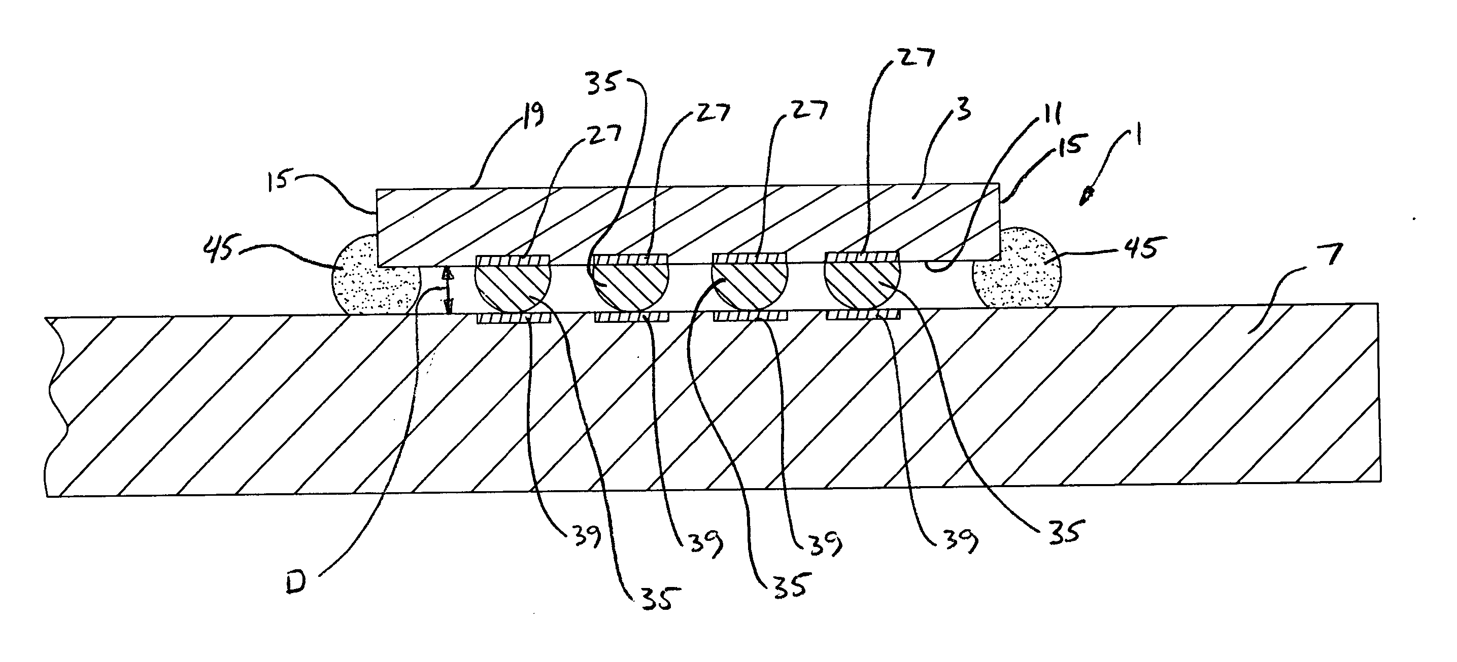
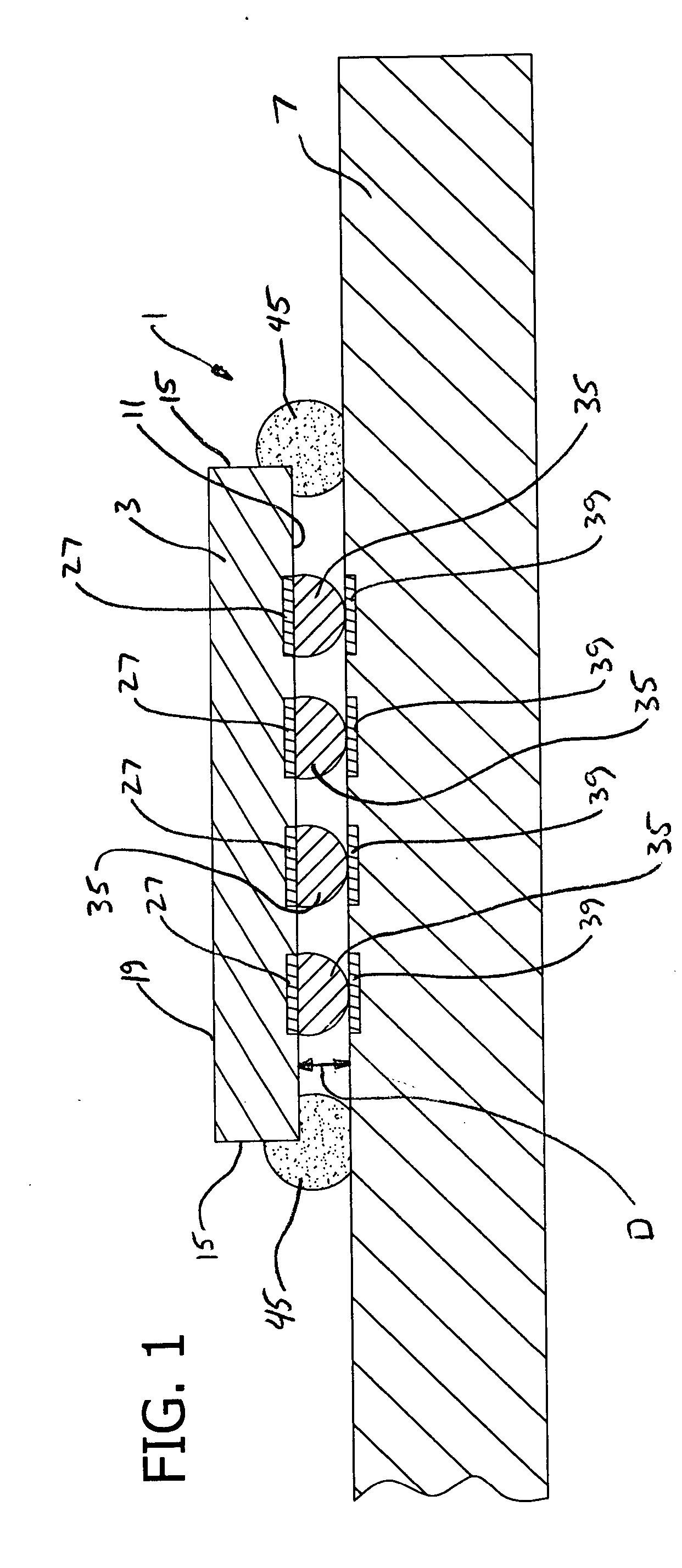
[0016] Referring now to the drawings, and more particularly to FIG. 1, an electrical circuit assembly, generally designated 1, comprises an integrated circuit (IC) device 3 assembled in accordance with the present invention. In the particular embodiment of FIG. 1, the IC device 3 is electrically and mechanically attached to a substrate 7 in the form of a printed circuit board of an electronic device (not shown). It will be understood that the circuit device 3 could be attached to a chip carrier substrate or other conventional connecting substrates (e.g., a pin-grid array or a land grid array) without departing from the scope of this invention. Also, the assembly 1 could include more than one IC device 3 assembled in accordance with the present invention.

[0017] In the illustrated embodiments, the IC device 3 is shown schematically but it will be understood that each device could comprise any typical IC device such as a Micro-Electronic Mechanical Systems (MEMS) device, Optoelectroni...


PUM

PropertyMeasurementUnit
bonding temperatureaaaaaaaaaa
heightaaaaaaaaaa

Abstract

An assembly of the present invention includes a substrate and an integrated circuit device adapted to be electrically and mechanically attached to the substrate. Electrically conductive connecting elements between the device and the substrate electrically connect the device and the substrate. At least one adhesive body is positioned between the integrated circuit device and the substrate to form a mechanical connection between the circuit device and the substrate. The at least one adhesive body comprises a non-thermosetting material which, when heated, releases said mechanical connection to allow removal of the circuit device from the substrate.

Description

BACKGROUND OF THE INVENTION [0001] The present invention relates generally to an electrical circuit assembly, and more particularly to a mechanical connection between a microchip and a substrate. [0002] Small portable electronic devices such as cellular phones contain various integrated circuit devices (i.e., microchips, chips, or dies) that are electrically and mechanically connected to a substrate (e.g., printed circuit board) to form an integrated circuit that controls the operation of the device. Portable electronic devices must withstand operation in rugged environments and sustain impact forces resulting from frequent dropping of the devices without failure of the integrated circuit. Prior to shipment of the finished electronic device, electronic manufacturers typically perform a drop test on the final assembly of the device to test the attachment force of the integrated circuit components to the circuit board. To pass the drop test, the finished product must withstand being d...

Claims


Application Information

Patent Timeline
Patent Type & Authority Applications(United States)
IPC IPC(8): H01L21/60H05K3/30
CPCH01L24/81H01L2224/83101H01L2224/81906H01L2224/81862H01L2224/81815H01L2224/811H01L2224/1703H01L2224/16227H01L2224/83194H01L2224/83856H01L2924/01079H01L2924/14H05K3/305H05K2201/0129H05K2201/10734H05K2203/0126H05K2203/0545H05K2203/176H01L24/75H01L2924/01005H01L2924/01006H01L2924/01033H01L2924/01075H01L2924/014H01L2224/16225H01L2224/81136H01L2224/81191H01L2224/17517H01L2224/17505H01L24/17H01L2224/131H01L2224/1319H01L2924/00014H01L2924/351H01L2924/12042H01L2224/05571H01L2224/05573Y02P70/50H01L2924/00H01L2224/05599
Inventor GILLEO, KENNETH B.
Owner COOKSON ELECTRONICS INC
Learn More