Plasma display panel

a technology of display panel and plasma, which is applied in the direction of discharge tube luminescnet screen, instrument, electrode, etc., can solve the problems of increasing the voltage for maintaining a discharge, increasing the abrasion of the front panel electrode, and time delay phenomenon, so as to increase brightness and efficiency, the effect of reducing the amount of erroneous discharge in each cell

Inactive Publication Date: 2005-03-17
LG ELECTRONICS INC
View PDF5 Cites 3 Cited by
  • Summary
  • Abstract
  • Description
  • Claims
  • Application Information

AI Technical Summary

Benefits of technology

[0025] According to the present invention, in a plasma display panel of a long column structure, it is possible lower a discharge start voltage and a discharge sustain voltage and to increase brightness and efficiency. Furthermore, color temperature equilibrium can be maintained every RGB cell and an erroneous discharge in each cell can be reduced.

Problems solved by technology

However, there are adverse effects in that abrasion of a front panel electrode increases and a sustain voltage for maintaining a discharge increases.
Thus, a time delay phenomenon that the start of a discharge is delayed occurs.
Therefore, there are problems in that a voltage for maintaining a discharge of a discharge space increases and a discharge start voltage rises.
In this case, there is a problem in that overall driving efficiency is lowered since an erroneous discharge occurs in the RGB cells.

Method used


Image

  • Plasma display panel
  • Plasma display panel
  • Plasma display panel

Examples


first embodiment

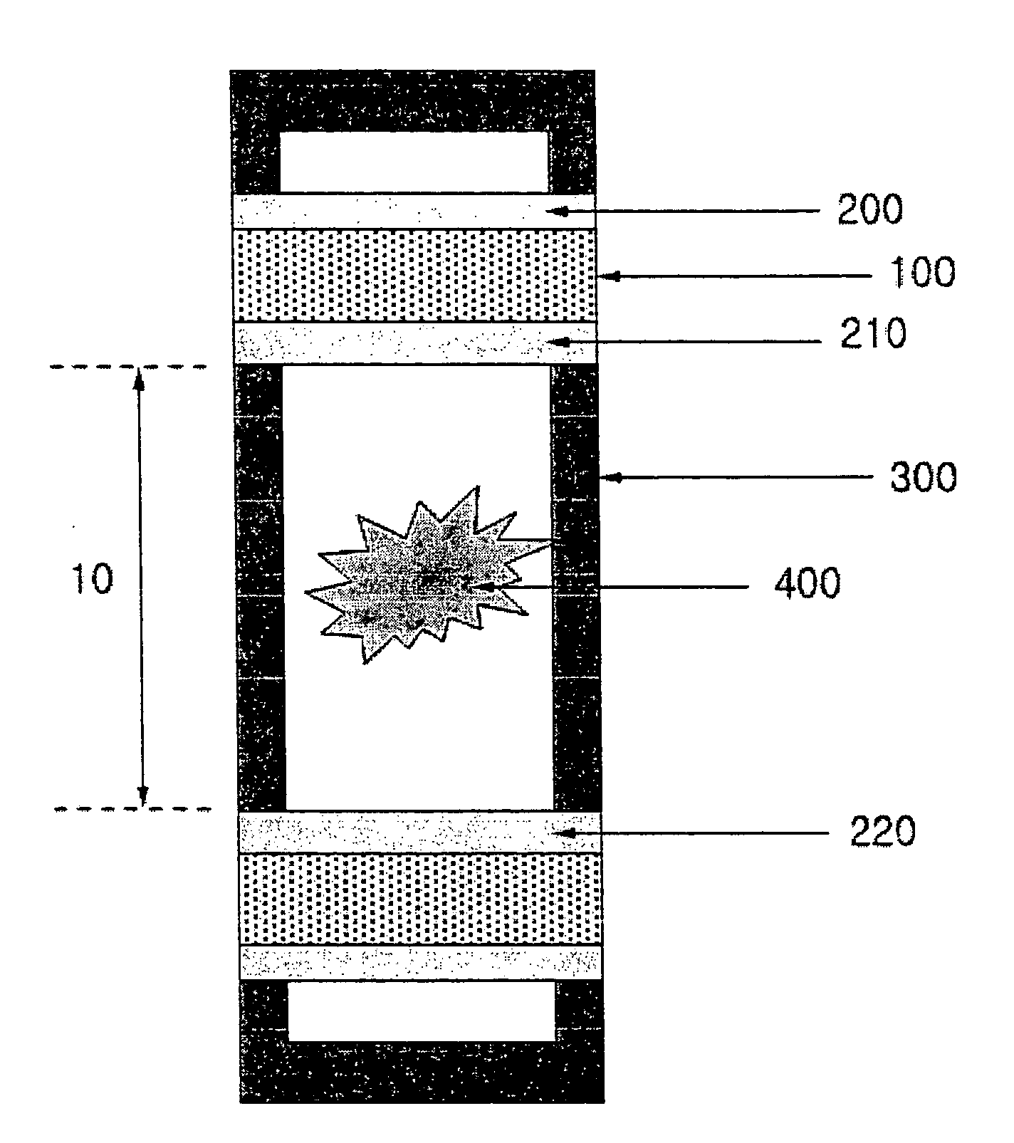
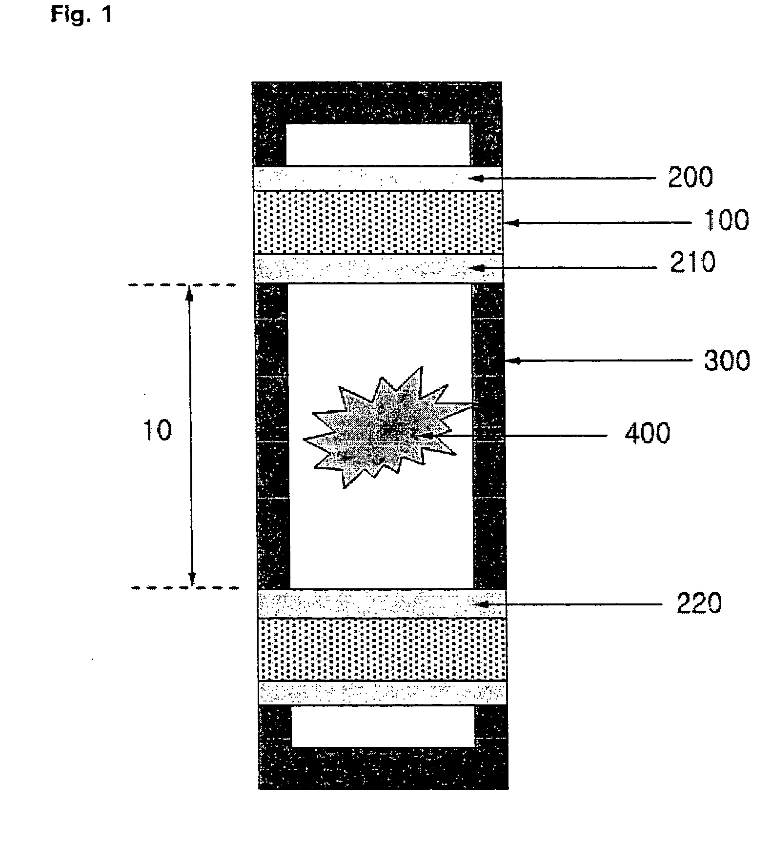
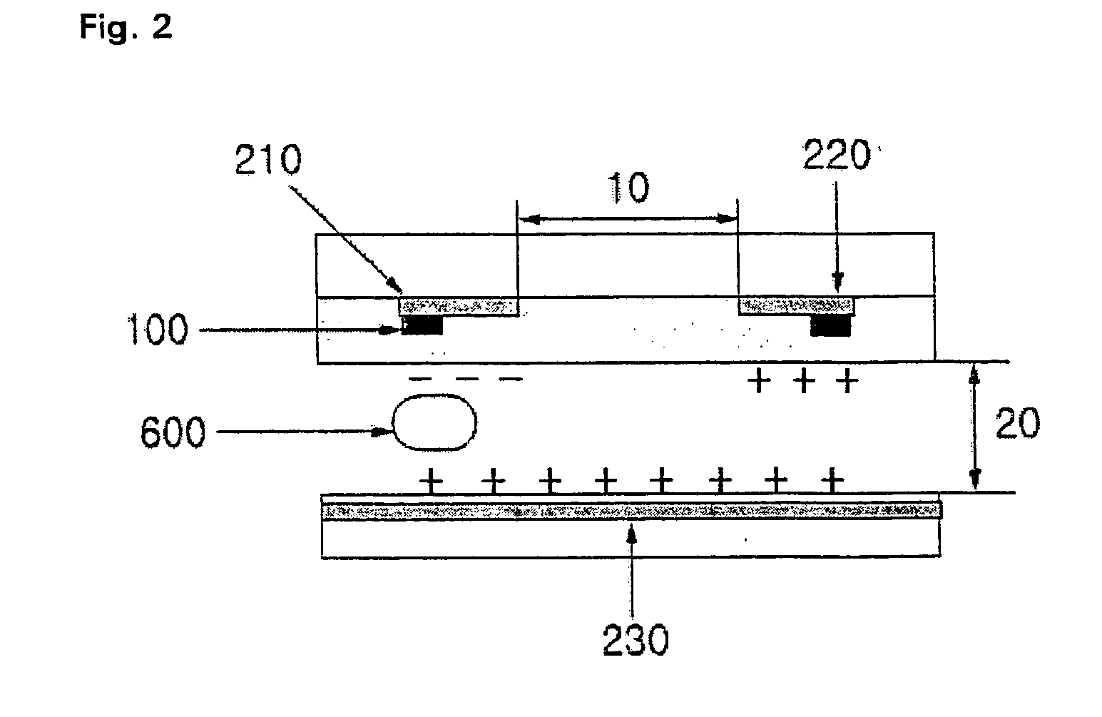
[0040] A plasma display panel according to a first embodiment of the present invention includes a front substrate and a rear substrate that are opposite to each other, wherein the plasma display panel includes scan electrodes and sustain electrodes that are spaced apart from each other in parallel on the opposite surface of the front substrate and have transparent electrodes and metal electrodes, respectively, a dielectric layer that covers the scan electrodes and the sustain electrodes, a protection film coated on the dielectric layer, address electrodes formed on the opposite surface of the rear substrate, a dielectric layer that covers the address electrodes, barrier ribs formed on the dielectric layer, discharge cells demarcated by the barrier ribs, and a phosphor layer coated on the inside of the discharge cells, wherein a distance between the scan electrodes and the sustain electrodes is greater than that between the front substrate and the rear substrate, wherein the transpar...

second embodiment

[0058] A plasma display panel according to a second embodiment of the present invention includes a front substrate and a rear substrate that are opposite to each other, wherein the plasma display panel includes scan electrodes and sustain electrodes that are spaced apart from each other in parallel on the opposite surface of the front substrate and have transparent electrodes and metal electrodes, respectively, a dielectric layer that covers the scan electrodes and the sustain electrodes, a protection film coated on the dielectric layer, address electrodes formed on the opposite surface of the rear substrate, a dielectric layer that covers the address electrodes, barrier ribs formed on the dielectric layer, discharge cells demarcated by the barrier ribs, and a phosphor layer coated on the inside of the discharge cells, wherein a distance between the scan electrodes and the sustain electrodes is greater than that between the front substrate and the rear substrate, wherein the transpa...

third embodiment

[0076] A plasma display panel according to a third embodiment of the present invention includes a front substrate and a rear substrate that are opposite to each other, wherein the plasma display panel includes scan electrodes and sustain electrodes that are spaced apart from each other in parallel on the opposite surface of the front substrate and have transparent electrodes and metal electrodes, respectively, a dielectric layer that covers the scan electrodes and the sustain electrodes, a protection film coated on the dielectric layer, address electrodes formed on the opposite surface of the rear substrate, a dielectric layer that covers the address electrodes, barrier ribs formed on the dielectric layer, discharge cells demarcated by the barrier ribs, and a phosphor layer coated on the inside of the discharge cells, wherein a distance between the scan electrodes and the sustain electrodes is greater than that between the front substrate and the rear substrate, wherein floating tra...


PUM


Abstract

The present invention relates to a plasma display panel, and more particularly, to an electrode structure of a plasma display panel capable of improving brightness and efficiency. According to a first embodiment of the present invention, in a plasma display panel of a long column structure having a front substrate and a rear substrate that are opposite to each other, the transparent electrodes of the scan electrodes or the sustain electrodes include projections projected toward the center of the discharge cells every discharge cell. Also, a discharge start voltage and a discharge sustain voltage can be lowered and brightness and efficiency can be increased. It is also possible to maintain color temperature equilibrium every RGB cell and to reduce an erroneous discharge of each cell.

Description

[0001] This Nonprovisional application claims priority under 35 U.S.C. § 119(a) on Patent Application No. 10-2003-0060885 filed in Korea on Sep. 1, 2003, Application No. 10-2004-0032393 filed in Korea on May 7, 2004 and Application No. 10-2004-0040548 filed in Korea on Jun. 3, 2004, the entire contents of which are hereby incorporated by reference. BACKGROUND OF THE INVENTION [0002] 1. Field of the Invention [0003] The present invention relates to a plasma display panel, and more particularly, to an electrode structure of a plasma display panel capable of improving brightness and efficiency. [0004] 2. Description of the Background Art [0005] Generally, in a plasma display panel (hereinafter, referred to as ‘PDP’), barrier ribs formed between a front glass and a rear glass made of soda lime glass constitute a single unit cell. When an inert gas having a small amount of xenon (Xe) added thereto is discharged by a high frequency voltage using neon (Ne), helium (He) or a mixed gas (Ne+H...

Claims


Application Information

Patent Timeline
Patent Type & Authority Applications(United States)
IPC IPC(8): H01J11/12H01J11/22H01J11/24H01J11/26H01J11/34
CPCH01J11/12H01J11/24H01J2211/326H01J2211/245H01J11/30
Inventor PARK, JAE BUMCHOI, SUNG CHUN
Owner LG ELECTRONICS INC
Why Eureka
Try Eureka