

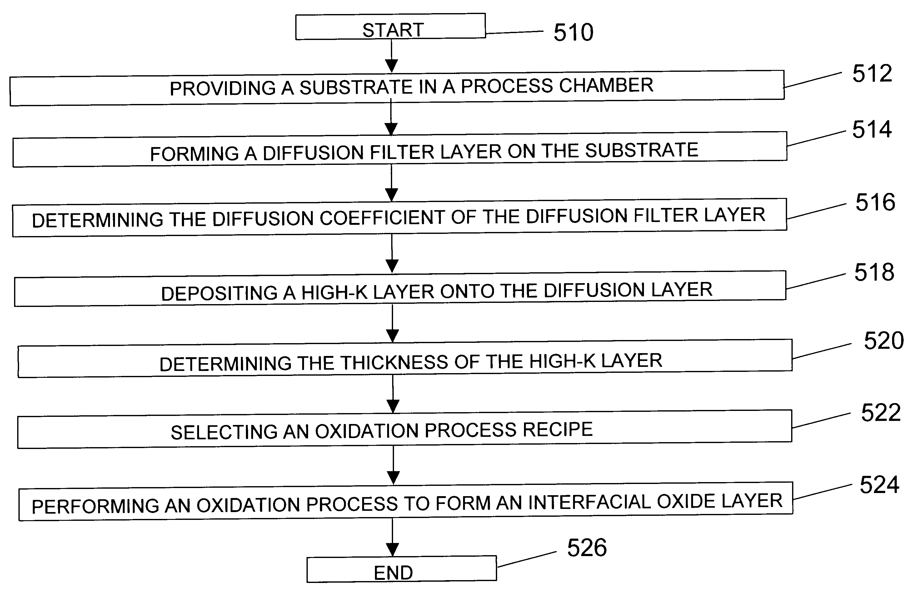
Interfacial oxidation process for high-k gate dielectric process integration
a dielectric process and interfacial oxidation technology, applied in the field of semiconductor processing, can solve the problems of imposing scaling constraints on the gate dielectric material, the overall dielectric constant of the microstructure, and the need to thin the oxide interfacial layer,
- Summary
- Abstract
- Description
- Claims
- Application Information
AI Technical Summary
Benefits of technology
Problems solved by technology
Method used
Image

Examples
Embodiment Construction
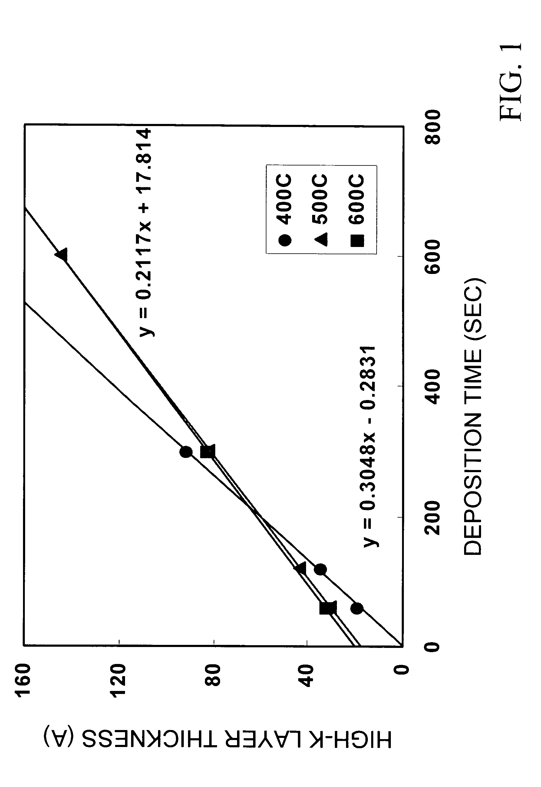
[0020]FIG. 1 shows the thickness of a high-k layer deposited by a TCVD process on a Si substrate as a function of deposition time. A thin native oxide layer was removed from the Si substrate by a wet cleaning process using HF, prior to depositing a high-k layer on the Si substrate. A HfO2 high-k layer was deposited on the clean Si substrate at substrate temperatures of 400° C., 500° C, and 600° C. The HfO2 layer was deposited by a TCVD process utilizing a process gas comprising a Hf(OBut)4 precursor.
[0021] In FIG. 1, the thickness of the HfO2 high-k layers as a function of deposition time was fitted using linear fits of the data points. The linear relationship between the high-k layer thickness and the deposition time for the 400° C. deposition curve, along with an intercept that goes through the origin, indicates minimal growth of an interfacial oxide layer between the high-k layer and the Si substrate. However, the intercepts for the 500° C. and 600° C. deposition curves indicate...
PUM
 Abstract
Description
Claims
Application Information