Arithmetic built-in self-test of multiple scan-based integrated circuits

a technology of integrated circuits and self-tests, applied in the field of integrated circuit testing, can solve the problems of reducing the area and performance of an integrated circuit, increasing latency, and excessive delays of high-speed ics used, and achieve the effect of reducing the impact of an error compensation phenomenon

Inactive Publication Date: 2005-03-17
MENTOR GRAPHICS CORP
View PDF23 Cites 31 Cited by
  • Summary
  • Abstract
  • Description
  • Claims
  • Application Information

AI Technical Summary

Benefits of technology

In accordance with yet another aspect of the present invention, the IC is further provided with microcode that implements an arithmetic test response compactor, which when executed by the embedded processor core, compacts

Problems solved by technology

However, this solution compromises an IC's area and performance as it inevitably introduces either a hardware overhead or additional delays and increased latency.
These delays may be excessive for high-speed ICs used in several applications such as high-performance microprocessors, digital signal processing (DSP) systems, new generations of floating point processors, and others.
The solutions range from pseudo-random techniques that do not use any storage (for test data) but take a long application time and often do not detect some faults to deterministic techniques that may require significant storage but achieve complete fault coverage in a relatively short time.
A common drawback of the sca

Method used


Image

  • Arithmetic built-in self-test of multiple scan-based integrated circuits
  • Arithmetic built-in self-test of multiple scan-based integrated circuits
  • Arithmetic built-in self-test of multiple scan-based integrated circuits

Examples


Embodiment Construction

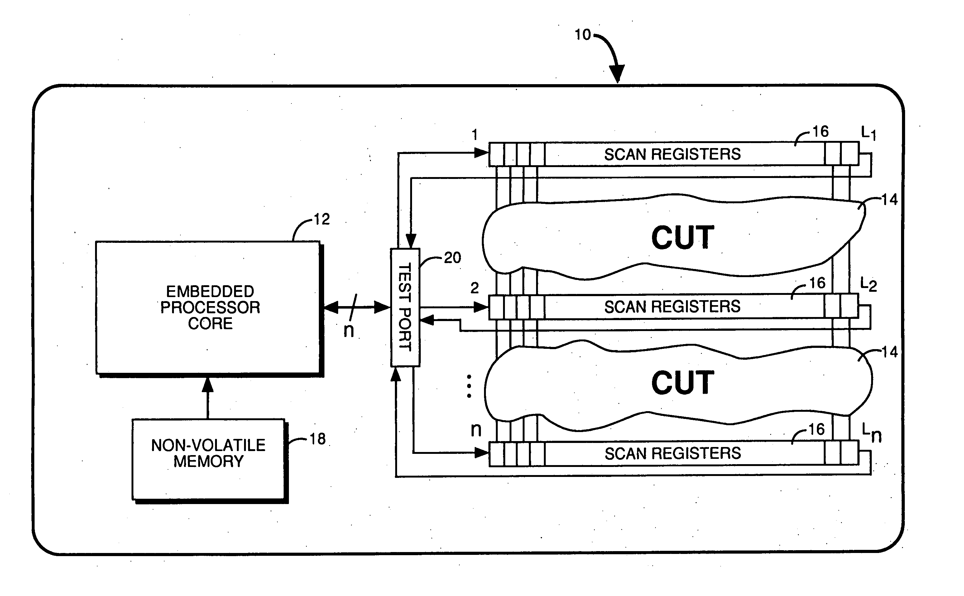
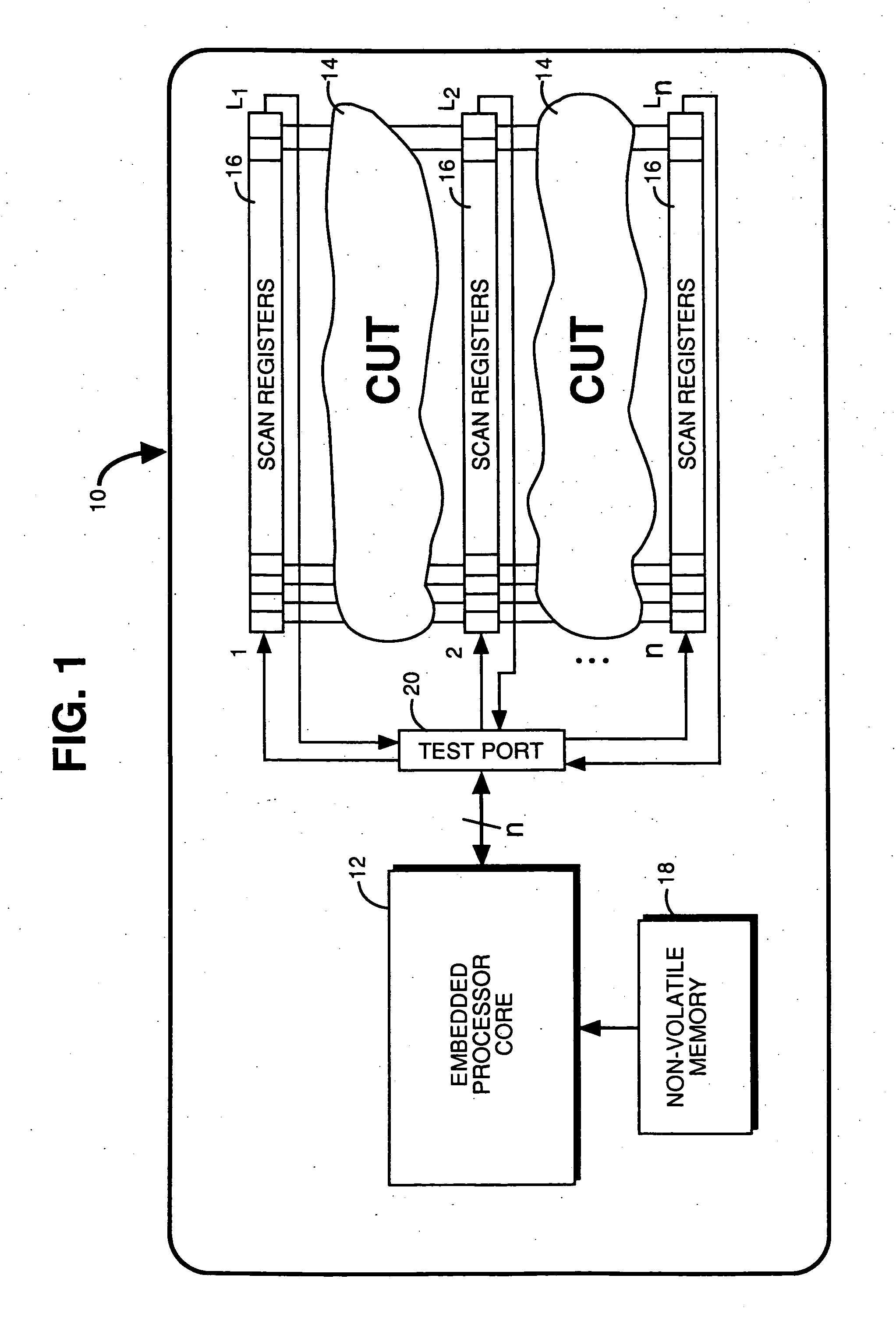
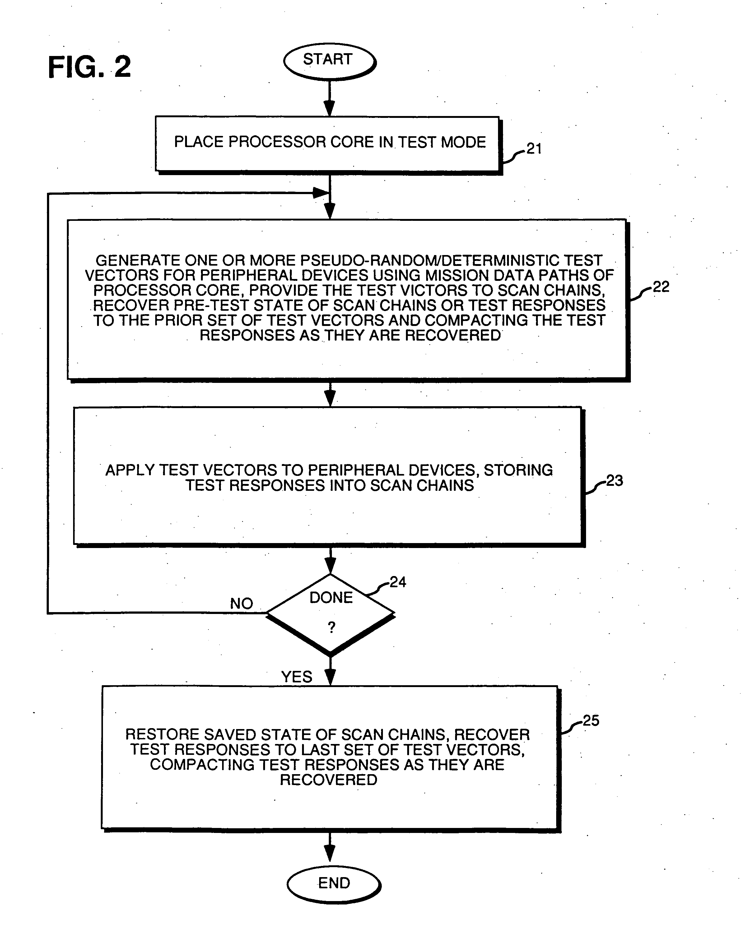
In the following description, various aspects of the present invention will be described. However, it will be apparent to those skilled in the art that the present invention may be practiced with only some or all aspects of the present invention. For purposes of explanation, specific numbers, materials and configurations are set forth in order to provide a thorough understanding of the present invention. However, it will also be apparent to one skilled in the art that the present invention may be practiced without the specific details. In other instances, well known features are omitted or simplified for clarity.

Parts of the description will be presented in terms of operations performed inside an integrated circuit with an embedded processor core and peripheral devices, using terms such as data, bits, values, numbers and the like, consistent with the manner commonly employed by those skilled in the art to convey the substance of their work to others skilled in the art. As well un...


PUM


Abstract

In one embodiment, an IC with an embedded processor core, peripheral devices, and associated multiple scan chains, is provided with microcode that implements an arithmetic pseudo-random number generator and an arithmetic deterministic test vector generator, when executed by the embedded processor core, generates 2-D pseudo-random and deterministic test vectors for testing the peripheral devices respectively. The IC is further provided with microcode that implements an arithmetic test response compactor, which when executed by the embedded processor core, compacts test responses of the peripheral devices into a signature. The IC further includes a test port register and microcode that implements a number of ABIST instructions.

Description

BACKGROUND OF THE INVENTION 1. Field of the Invention The present invention relates generally to testing of integrated circuits (IC) and more particularly to arithmetic built-in self-test (ABIST) of multiple scan-based ICs. 2. Background Information Many ICs are produced in large volume and very often operate at high speeds. Since their manufacturing yield strongly depends on the silicon area, and their performance is directly related to the delays on critical paths, it is essential that the testing strategy provides a high fault coverage without a significant area overhead and performance degradation. As the costs associated with detecting faults rise over thousands of times from the time ICs are fabricated to the time the final product is released to customers, the most effective way to prevent costly rework is to consider testing issues as early in the design cycle as possible. Practical importance of this problem in conjunction with the increasing complexity of VLSI circuits...

Claims


Application Information

Patent Timeline
IPC IPC(8): G01R31/3185G06F11/267
CPCG01R31/318385G06F11/2221G01R31/318547
Inventor RAJSKI, JANUSZTYSZER, JERZY
Owner MENTOR GRAPHICS CORP
Why Eureka
Try Eureka