A1/A1Ox/A1 resistor process for integrated circuits

a technology of resistors and integrated circuits, applied in resistor manufacturing, semiconductor devices, resistors, etc., can solve the problems of reducing the quantity and value of resistors, consuming much chip area of shunting resistors, and adding circuit parasitic inductance,

Inactive Publication Date: 2005-03-24
NORTHROP GRUMAN CORP
View PDF25 Cites 26 Cited by
  • Summary
  • Abstract
  • Description
  • Claims
  • Application Information

AI Technical Summary

Problems solved by technology

In such a configuration, the shunting resistor consumes much of the chip area and adds to the parasitic inductance of the circuit.
However, there are problems associated with such vertical resistors in these applications.
As is known in the art, the cleaning process significantly reduces the quantity and value of the resistor.

Method used


Image

  • A1/A1Ox/A1 resistor process for integrated circuits
  • A1/A1Ox/A1 resistor process for integrated circuits
  • A1/A1Ox/A1 resistor process for integrated circuits

Examples


Embodiment Construction

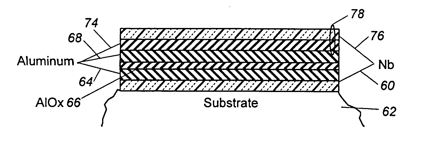
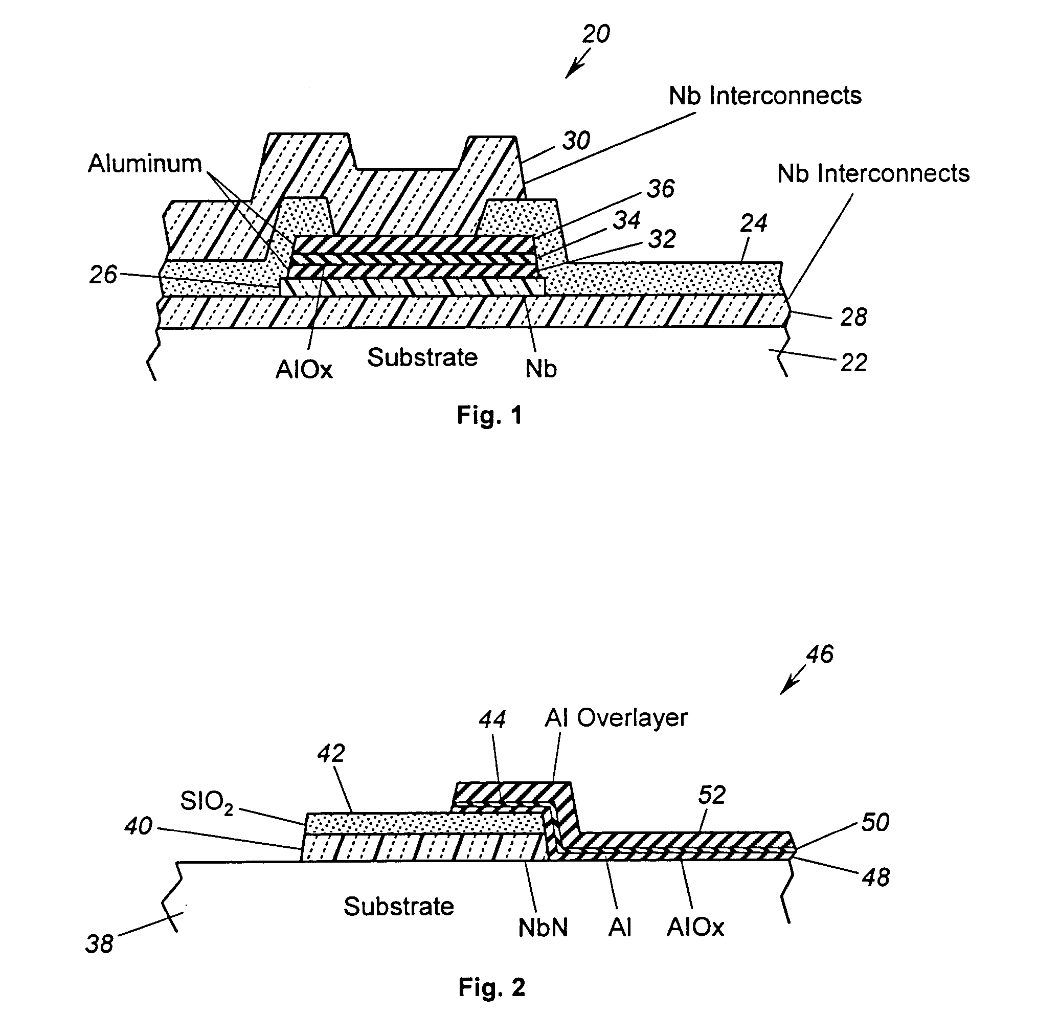
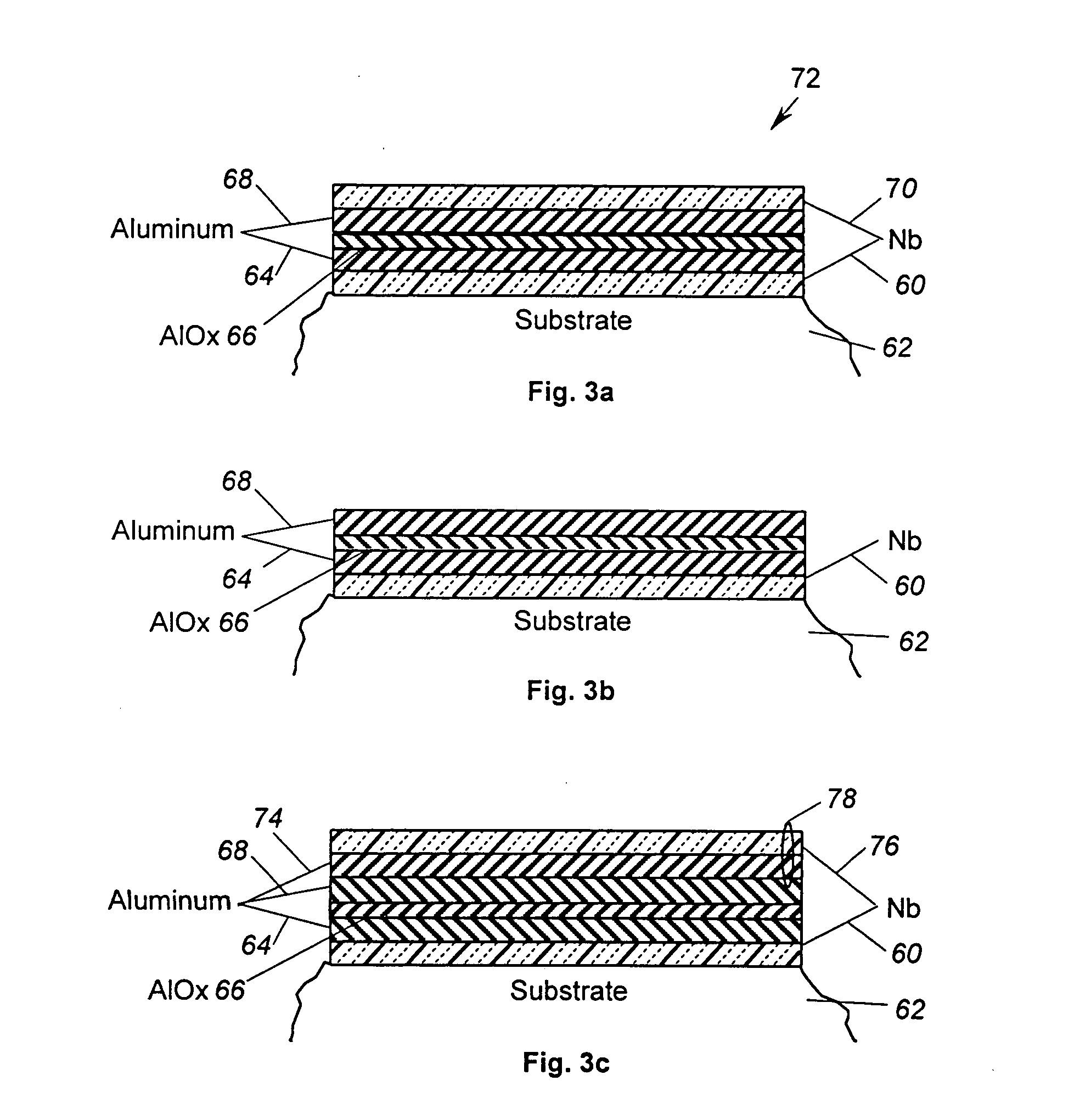
[0014] The present invention relates to a vertical resistance structure for use with integrated circuits which include superconducting junctions or films. An example of such an integrated circuit structure is disclosed in commonly owned U.S. Pat. No. 5,892,243, hereby incorporated by reference. Such circuits have been known to employ shunting resistors formed as vertical resistance structures. An example of a known superconducting circuit utilizing vertical shunting resistors is disclosed in: P. Wolf, “Use of Paramagnetic or Other Impurities in Josephson Technology”, IBM Technical Disclosure Bulletin, Vol. 18, No. 8, January 1976, page 2645. As discussed above, the resistance structure is normally cleaned prior to the deposition of the interconnect material which results in a resistance that is a function of the uniformity of the thickness of the material across the wafer. The present invention solves this problem by utilizing a material system in which the cleaning process has a ne...


PUM

PropertyMeasurementUnit
resistancesaaaaaaaaaa
thickaaaaaaaaaa
thickaaaaaaaaaa

Abstract

A structure and a method for forming a vertical resistor on a superconducting integrated circuit. The resistance structure is formed from a Al / AlOx / Al material system. In particular, the resistance structure includes a layer of aluminum, in-situ oxidation of the aluminum surface and further deposition of aluminum. The resistance of the Al / AlOx / Al structure primarily comes from the aluminum oxide layer rather than the aluminum. As such, any aluminum removed during the interconnect pre-cleaning process will have a negligible impact on the overall resistance of the structure.

Description

BACKGROUND OF THE INVENTION [0001] 1. Field of the Invention [0002] The present invention relates to superconducting devices and more particularly to a method for forming a vertical resistor on an integrated circuit, for example, a superconducting integrated circuit, using Al / AlOx / Al, which not only reduces the chip area of the resistor but provides across wafer uniformity as a function of the self-limiting oxidation of the aluminum and is not a strong function of the deposition uniformity since the spreading resistance effects occur in a relatively low resistance portion of the resistor structure and thus has a negligible effect on the overall resistance. [0003] 2. Description of the Prior Art [0004] Integrated circuits formed with superconducting junctions are generally known in the art. An example of such an integrated circuit is disclosed in commonly owned U.S. Pat. No. 5,892,243, hereby incorporated by reference. Such superconducting junctions are known as Josephson junctions. ...

Claims


Application Information

Patent Timeline
Patent Type & Authority Applications(United States)
IPC IPC(8): H01C7/00H01C17/075H01L27/18
CPCH01C7/006H01L27/18H01C17/075H10N69/00
Inventor MURDUCK, JAMES MATTHEWSILVER, ARNOLD HERBERT
Owner NORTHROP GRUMAN CORP
Why Eureka
Try Eureka