Wiring optimization method and device of superconducting integrated circuit, storage medium and terminal

An integrated circuit and wiring technology, applied in the field of superconducting integrated circuit layout, can solve the problems of being unable to apply high-scale superconducting integrated circuits, taking a long time, and affecting the design iteration cycle of superconducting integrated circuits, so as to reduce design time overhead and be compatible Good performance and reduced design cost

Active Publication Date: 2021-12-10
SHANGHAI INST OF MICROSYSTEM & INFORMATION TECH CHINESE ACAD OF SCI
View PDF9 Cites 4 Cited by
  • Summary
  • Abstract
  • Description
  • Claims
  • Application Information

AI Technical Summary

Problems solved by technology

[0005] The technical problem to be solved by the present invention is that there are still a large number of manual design processes in the existing superconducting integrated circuit wiring method, which takes a long time, seriously affects the design iteration cycle of superconducting integrated circuits, and cannot be applied to high-scale superconducting integrated circuits

Method used


Image

  • Wiring optimization method and device of superconducting integrated circuit, storage medium and terminal
  • Wiring optimization method and device of superconducting integrated circuit, storage medium and terminal
  • Wiring optimization method and device of superconducting integrated circuit, storage medium and terminal

Examples


Embodiment 1

[0055] In order to solve the technical problems existing in the prior art, an embodiment of the present invention provides a wiring optimization method for a superconducting integrated circuit.

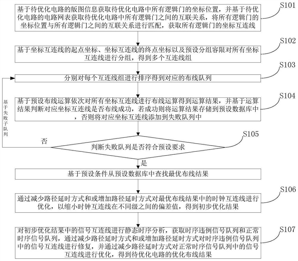
[0056] figure 1 A schematic flow chart showing a wiring optimization method for a superconducting integrated circuit according to an embodiment of the present invention; refer to figure 1 As shown, the wiring optimization method for a superconducting integrated circuit in the embodiment of the present invention includes the following steps.

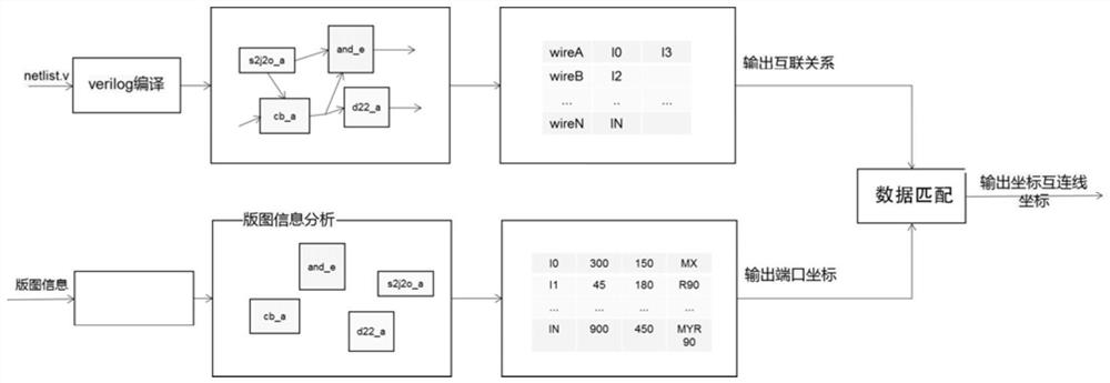
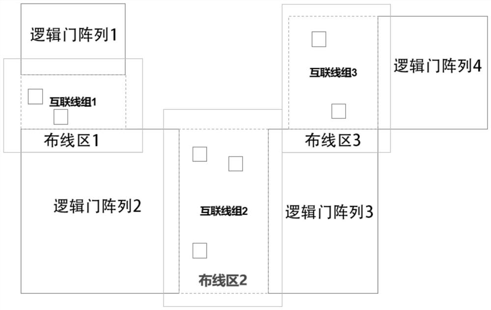
[0057] In step S101, the coordinate positions of all logic gates in the circuit to be optimized are obtained based on the layout information of the circuit to be optimized, and the interconnection relationship between all logic gates in the circuit to be optimized is obtained based on the circuit netlist of the circuit to be optimized. The coordinate position is matched with the interconnection relationship between all logic gates, and the coord...

Embodiment 2

[0088] In order to solve the above-mentioned technical problems existing in the prior art, an embodiment of the present invention also provides a wiring optimization device for a superconducting integrated circuit.

[0089] Figure 12 It shows a schematic structural diagram of a wiring optimization device for a superconducting integrated circuit in Embodiment 2 of the present invention; refer to Figure 12 As shown, the wiring optimization device for a superconducting integrated circuit according to the embodiment of the present invention includes a coordinate interconnection acquisition module, a wiring operation module, an optimal wiring result acquisition module, a clock optimization module, and a wiring optimization module.

[0090] The coordinate interconnection acquisition module is used to obtain the coordinate positions of all logic gates in the circuit to be optimized based on the layout information of the circuit to be optimized, and obtain the interconnection relati...

Embodiment 3

[0097] In order to solve the above-mentioned technical problems existing in the prior art, the embodiment of the present invention also provides a storage medium, which stores a computer program, and when the computer program is executed by a processor, the wiring optimization of the superconducting integrated circuit of the first embodiment can be realized all steps in the method.

[0098] The specific steps of the method for optimizing the wiring of a superconducting integrated circuit and the beneficial effects obtained by using the readable storage medium provided by the embodiment of the present invention are the same as those of the first embodiment, and will not be repeated here.

[0099] It should be noted that the storage medium includes various media capable of storing program codes such as ROM, RAM, magnetic disk or optical disk.


PUM


Abstract

The invention discloses a wiring optimization method and device for a superconducting integrated circuit, a storage medium and a terminal. The method comprises the steps: obtaining logic gate coordinate interconnection lines based on the layout information of a to-be-optimized circuit and a circuit netlist, carrying out the wiring operation of all coordinate interconnection lines, and storing the operation result of successful wiring in a preset database, adding the coordinate interconnection line corresponding to the wiring failure into a failure queue; obtaining an optimal wiring result based on the failure queue; and optimizing the clock interconnection line and the signal interconnection line in the optimal wiring result based on a path delay reducing mode and/or a path delay increasing mode to obtain an optimized wiring result of the to-be-optimized circuit. According to the method, the automatic wiring problem after the superconducting integrated circuit is arranged is solved, the design cost is reduced, and the design time overhead caused by manual wiring is reduced.

Description

technical field [0001] The invention relates to the technical field of layout of superconducting integrated circuits, in particular to a method and device for optimizing wiring of superconducting integrated circuits, a storage medium and a terminal. Background technique [0002] Superconducting integrated circuits refer to integrated circuits based on Josephson junctions and superconducting materials, including Single-Flux-Quantum (SFQ) circuits. [0003] SFQ circuit is a relatively special superconducting integrated circuit, which is mainly composed of Josephson junctions, and the digital logic "0" and "1" are represented by the presence or absence of magnetic flux quantum Ф0. Compared with traditional semiconductor CMOS (Complementary MetalOxide Semiconductor) circuits, the tiny and quantized nature of the magnetic flux quantum significantly reduces the influence of crosstalk and power consumption, and the narrow voltage pulse generated in the junction when the magnetic fl...

Claims


Application Information

Patent Timeline
Patent Type & Authority Applications(China)
IPC IPC(8): G06F30/394
CPCG06F30/394
Inventor 杨树澄任洁高小平王镇
Owner SHANGHAI INST OF MICROSYSTEM & INFORMATION TECH CHINESE ACAD OF SCI
Why Eureka
Try Eureka